Particle monitoring method of wet cleaning process apparatus

A technology of process equipment and wet cleaning, which is applied in the fields of electrical components, semiconductor/solid-state device manufacturing, circuits, etc., and can solve problems such as difficulty in taking into account high sensitivity and accuracy

Active Publication Date: 2014-12-10
SHANGHAI HUALI MICROELECTRONICS CORP
View PDF4 Cites 2 Cited by
  • Summary
  • Abstract
  • Description
  • Claims
  • Application Information

AI Technical Summary

Problems solved by technology

[0004] However, it is difficult to be detected by defect detection due to the adsorption of very small particles in the acid bath to the wafer, such as figure 1 The small particles 10 shown are attached to the wafer 20 through the acid bath, and the distribution of the number of defects after the defect detection is normal as shown in FIG. figure 2 shown
However, after the surface is covered with a thin film by chemical deposition growth, the size of the particles is enlarged by the subsequent growth film (such as image 3 Shown in the reference number 30), it is easy to be found by defect detection, and its defect detection result is as follows Figure 4 shown
[0005] However, imaging by transmission electron microscopy shows that the core of the defect is indeed located between the wafer surface and the grown film as Figure 5 As shown, although the introduction of subsequent processes can improve the ability of defect detection, it also introduces other factors that cause particles, so it is difficult to balance high sensitivity and high accuracy.

Method used


Image

  • Particle monitoring method of wet cleaning process apparatus
  • Particle monitoring method of wet cleaning process apparatus
  • Particle monitoring method of wet cleaning process apparatus

Examples


Embodiment Construction

[0024] In order to make the content of the present invention clearer and easier to understand, the content of the present invention will be described in detail below with reference to specific embodiments and drawings.

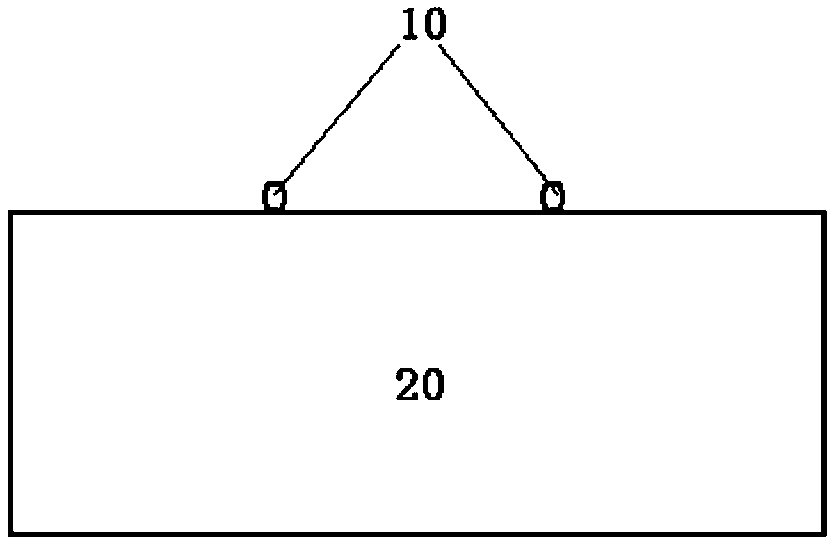
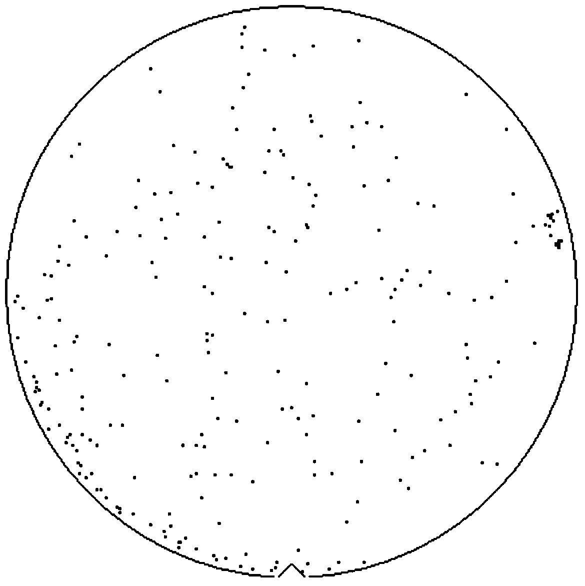
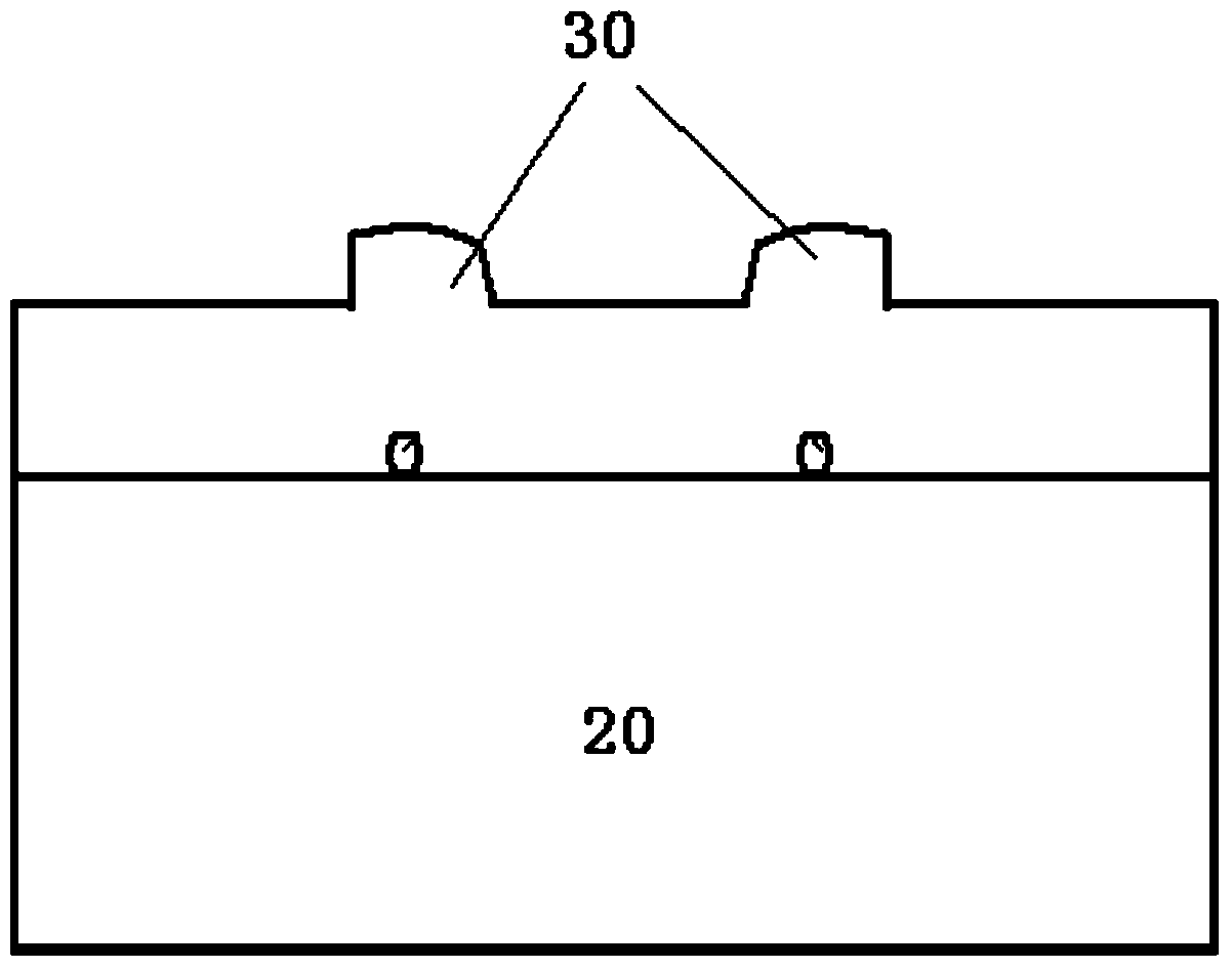
[0025] The method for monitoring particles of wet cleaning process equipment according to a preferred embodiment of the present invention includes: immersing a part of the wafer area of ​​the wafer in the chemical solution of the acid tank, and making another part of the wafer area of ​​the wafer expose the chemical in the acid tank. Liquid (that is, not immersed in the chemical liquid); cleaning a part of the wafer area immersed in the chemical liquid in the acid tank by simulating the cleaning process; after performing the cleaning, the entire wafer (that is, the part of the wafer area and the The other part of the wafer area) performs a thin film growth process; after the thin film growth process is performed, defects on the wafer are detected, and the wet proc...


PUM


Abstract

The invention provides a particle monitoring method of a wet cleaning process apparatus. The particle monitoring method comprises the steps of immersing one part of wafer region of a wafer into a liquor in an acid tank and keeping the other part of wafer region of the wafer exposed from the liquor in the acid tank, cleaning the part of wafer region immersed in the liquor in the acid tank through a simulation cleaning process, performing a film growth process on the whole wafer after cleaning, defecting defects on the wafer after the film growth process, and determining whether the wet process and the film growth process are abnormal according to the defect distribution on the one part of wafer region and the other part of wafer region.

Description

Technical field [0001] The present invention relates to the field of semiconductor manufacturing, and more specifically, the present invention relates to a method for monitoring particles of wet cleaning process equipment. Background technique [0002] The advanced integrated circuit manufacturing process generally includes several hundred steps. A small error in any link will lead to the failure of the entire chip. Especially as the critical size of the circuit continues to shrink, its requirements for process control become stricter. In order to find and solve problems in time during the production process, generally equipped with optical and electron beam defect detection equipment to conduct online products. [0003] However, on the one hand, the current online testing equipment is very expensive, and its investment cost is even higher than that of process equipment. On the other hand, when online inspection finds that there is an abnormality on the production line, it means t...

Claims


Application Information

Patent Timeline
Patent Type & Authority Applications(China)
IPC IPC(8): H01L21/02H01L21/66
CPCH01L22/12
Inventor 倪棋梁陈宏璘龙吟
Owner SHANGHAI HUALI MICROELECTRONICS CORP
Why Eureka
Try Eureka