Touch substrate, manufacturing method of touch substrate and touch display device

A technique for touching a substrate and a manufacturing method, which is applied in the directions of instruments, calculations, and electrical digital data processing, etc., and can solve problems such as easy occurrence of diffraction, reduced scanning frequency of the touch substrate, increased signal attenuation, etc., and achieves reduction of moire effect, The effect of reducing light diffraction and reducing the number of included angles

Inactive Publication Date: 2014-12-17
HEFEI XINSHENG OPTOELECTRONICS TECH CO LTD +1
View PDF5 Cites 24 Cited by
  • Summary
  • Abstract
  • Description
  • Claims
  • Application Information

AI Technical Summary

Problems solved by technology

But this approach is limited by the size
Because in the case of a large size, when the sensing electrode is made of indium tin oxide (ITO), the resistance of the sensing electrode is large, and the signal attenuation increases, making signal processing difficult. At the same time, the increase in resistance makes the scanning of the touch substrate difficult. frequency decrease
In order to prevent the large sensi

Method used


Image

  • Touch substrate, manufacturing method of touch substrate and touch display device
  • Touch substrate, manufacturing method of touch substrate and touch display device
  • Touch substrate, manufacturing method of touch substrate and touch display device

Examples


Embodiment Construction

[0040] Specific embodiments of the present invention will be described in detail below in conjunction with the accompanying drawings. It should be understood that the specific embodiments described here are only used to illustrate and explain the present invention, and are not intended to limit the present invention.

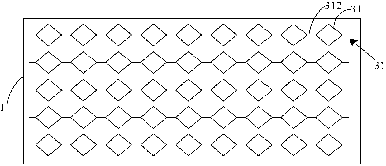
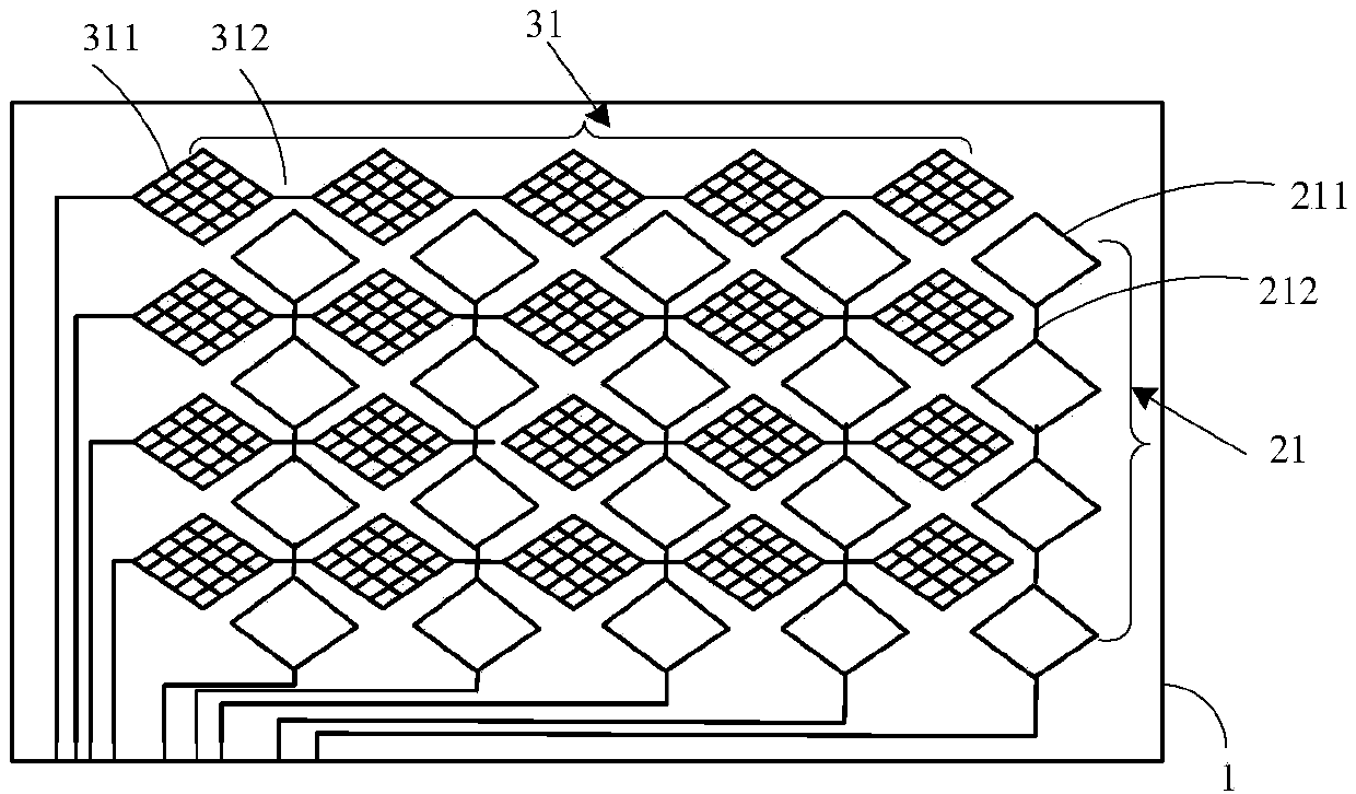
[0041] As a first aspect of the present invention, a touch substrate is provided, such as Figure 1 to Figure 3 As shown, the touch substrate includes a first electrode layer 2 and a second electrode layer 3 arranged on the base substrate 1, the first electrode layer 2 includes a plurality of first electrodes 21, and the second electrode layer 3 includes a plurality of The second electrode 31, each first electrode 21 includes a plurality of first electrode units 211 and a first connecting portion 212 connected between two adjacent first electrode units 211, each second electrode 31 includes a plurality of first electrode units 211 Two electrode units 311 and th...


PUM


Abstract

The invention provides a touch substrate, a manufacturing method of the touch substrate and a touch display device. The touch substrate comprises a first electrode layer and a second electrode layer which are arranged on a lining substrate, wherein the first electrode layer comprises a plurality of first electrodes; the second electrode layer comprises a plurality of second electrodes; each first electrode comprises a plurality of first electrode units and first connecting parts which are connected between two adjacent first electrode units; each second electrode comprises a plurality of second electrode units and second connecting parts which are connected between two adjacent second electrode units; the first connecting parts and the second connecting parts are intersected; the first electrode units are transparent electrode blocks; the second electrode units are metal grid electrode blocks. The total resistance of electrodes on the touch substrate can be reduced, the manufacturing method can be suitable for manufacturing the touch substrate with large size, and meanwhile, the ripple effect is reduced.

Description

technical field [0001] The present invention relates to the field of touch technology, in particular to a touch substrate, a manufacturing method of the touch substrate, and a touch display device including the touch substrate. Background technique [0002] As one of the most convenient human interaction technologies, touch technology has gradually penetrated into people's lives. The capacitive touch screen is an important form of the touch screen. The touch substrate of the capacitive touch screen includes a driving electrode layer and a sensing electrode layer. A plurality of driving electrodes of the driving electrode layer and a plurality of sensing electrodes of the sensing electrode layer cross each other. Capacitors are formed adjacent to the electrodes; each driving electrode is loaded with a driving signal in a scanning form, and a corresponding sensing signal is generated on the sensing electrode. The capacitance between them, so that the sensing signal of the cor...

Claims


Application Information

Patent Timeline
IPC IPC(8): G06F3/045
CPCG06F3/0445G06F3/0446G06F2203/04103G06F2203/04111G06F2203/04112
Inventor 丁贤林胡明
Owner HEFEI XINSHENG OPTOELECTRONICS TECH CO LTD
Why Eureka
Try Eureka