
A printed circuit board and an intelligent terminal

A printed circuit board and wire routing technology, which is applied in the field of electronic equipment, can solve the problems that smart terminals cannot meet the thinning requirements and large area, and achieve the effect of meeting the thinning requirements, reducing the number, and reducing the area

Inactive Publication Date: 2017-09-15
GUANGDONG OPPO MOBILE TELECOMM CORP LTD
View PDF6 Cites 0 Cited by
  • Summary
  • Abstract
  • Description
  • Claims
  • Application Information

AI Technical Summary

Problems solved by technology

[0004] In summary, a considerable area needs to be reserved on the printed circuit board of the main board of the smart terminal to place numerous test points and cursor alignment points, which makes the area of ​​the existing printed circuit board too large, which in turn leads to the The terminal cannot meet the thinning requirements

Method used


Image

  • A printed circuit board and an intelligent terminal
  • A printed circuit board and an intelligent terminal
  • A printed circuit board and an intelligent terminal

Examples


no. 1 example

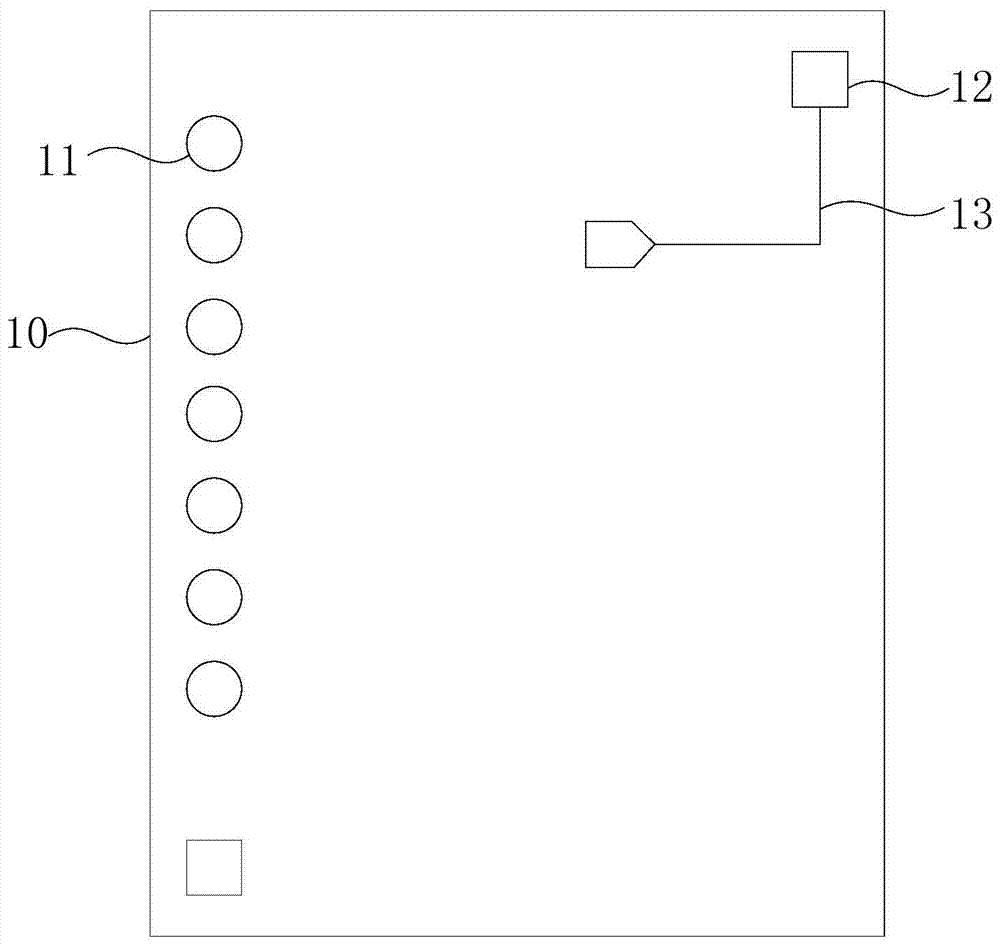
[0026] figure 1 is a schematic structural view of the printed circuit board provided in the first embodiment of the present invention. like figure 1 As shown, the printed circuit board includes an insulating substrate 10, on which a functional test line 13, a test point 11 and a cursor alignment point 12 are arranged, wherein at least one cursor alignment point 12 is compatible with the function The test trace 13 is electrically connected.

[0027] Wherein, each test point 11 in the printed circuit board is electrically connected to its corresponding functional test wiring 13, and the test point 11 is convenient for the test probe to conduct a functional test on the printed circuit board, such as the printed circuit board Check open circuit, short circuit and welding condition of all parts.

[0028] More than twenty test points may be included in the printed circuit board. For example, the printed circuit board of a smartphone can include the following test points11: 3 tes...

no. 2 example

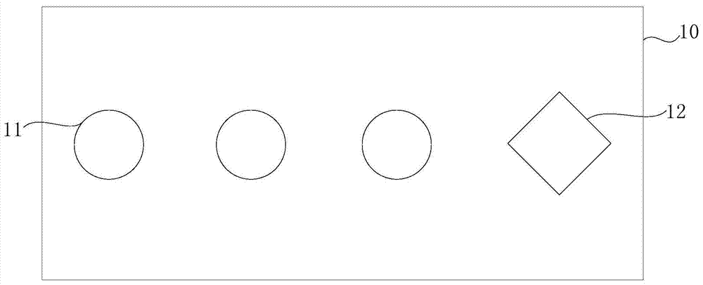
[0035] The printed circuit board provided in the second embodiment of the present invention includes an insulating substrate, and functional test wiring, test points, and cursor alignment points are arranged on the insulating substrate, wherein at least one cursor alignment point is aligned with the functional test Trace electrical connections.

[0036] Wherein, the printed circuit board may include a plurality of test points, and each test point is electrically connected to its corresponding functional test wiring, and the test points facilitate the conduction of the probes to realize the functional test of the printed circuit board.

[0037] Wherein, the front and back sides of the printed circuit board include two cursor alignment points respectively, that is, the printed circuit board includes four cursor alignment points in total, and the cursor alignment points provide a common possibility for all steps in the surface mount process. The measurement point ensures that the...

no. 3 example

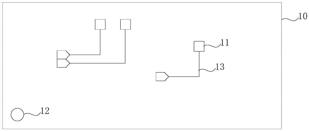
[0052] In the third embodiment of the present invention, the printed circuit board provided in the embodiment of the present invention is introduced by taking a printed circuit board including one cursor alignment point and capable of implementing three functional tests as an example. figure 2 is a structural schematic diagram of an existing printed circuit board, image 3 It is a schematic diagram of the circuit principle of the existing printed circuit board; Figure 4 is a schematic structural view of the printed circuit board provided in the third embodiment of the present invention, Figure 5 is a schematic diagram of the circuit principle of the printed circuit board provided in the third embodiment of the present invention.

[0053] combine figure 2 and image 3 As shown, in order to realize the three kinds of functional tests, three test points 11 need to be included in the existing printed circuit board, because the printed circuit board also includes a cursor al...


PUM


Abstract

The embodiment of the invention relates to the technical field of electronic equipment, in particular to a printed circuit board and an intelligent terminal. The printed circuit board comprises an insulation substrate, and the insulation substrate is provided with a function test wire, test points and cursor positioning points. At least one cursor positioning point is electrically connected with the function test wire. According to the printed circuit board, the number of the test points is reduced, so that the area of the printed circuit board is reduced, and the intelligent terminal comprising the printed circuit board meets the requirement for being thin.

Description

technical field [0001] The embodiments of the present invention relate to the technical field of electronic equipment, and in particular to a printed circuit board and an intelligent terminal. Background technique [0002] Printed Circuit Board (PCB) is the carrier of all electronic products. It installs various integrated circuits, components and connectors, and is interconnected by multi-layer wiring to form various electronic components. [0003] With the increasing automation of the smart terminal manufacturing process, more and more test points need to be set on the printed circuit board to detect the product yield of each production step in the manufacturing process. In addition, the printed circuit board also needs to include multiple cursor alignment points (Mark points) to meet the requirements of Surface Mounted Technology (SMT). In order to cooperate with the production and use of test fixtures, the size and spacing of each test point must meet certain requiremen...

Claims


Application Information

Patent Timeline
Patent Type & Authority Patents(China)
IPC IPC(8): H05K1/02G01R31/28G01R31/02
CPCG01R31/2812G01R31/2815H05K1/0266H05K1/0268
Inventor 彭飞
Owner GUANGDONG OPPO MOBILE TELECOMM CORP LTD
Learn More