Pressure-resistance structure of electronic device

A technology of electronic devices and electronic components, which is applied in the direction of electrical equipment structural parts, electrical components, casing/cabinet/drawer parts, etc., can solve the problems of LCM mechanical or optical damage, electronic component damage, etc., to achieve streamlining Quantity, convenient assembly, avoiding the effect of stress concentration

Active Publication Date: 2015-01-14
SHENXUN COMP KUNSHAN +1
View PDF5 Cites 0 Cited by
  • Summary
  • Abstract
  • Description
  • Claims
  • Application Information

AI Technical Summary

Problems solved by technology

[0004] However, the undulating groove or channel-like design on the case creates a protrusion on the inside of the case
The protruding part will give a concentrated stress to the electronic components in the casing, and cause the electronic components to be easily damaged after being stressed
Taking the Liquid Crystal Display Module (LCM) in a notebook computer as an example, the high and low undulating structure of the casing will make the local position of the LCM bear concentrated pressure (stress concentration), which will cause the LCM to be prone to mechanical or optical damage.

Method used


Image

  • Pressure-resistance structure of electronic device
  • Pressure-resistance structure of electronic device
  • Pressure-resistance structure of electronic device

Examples


Embodiment Construction

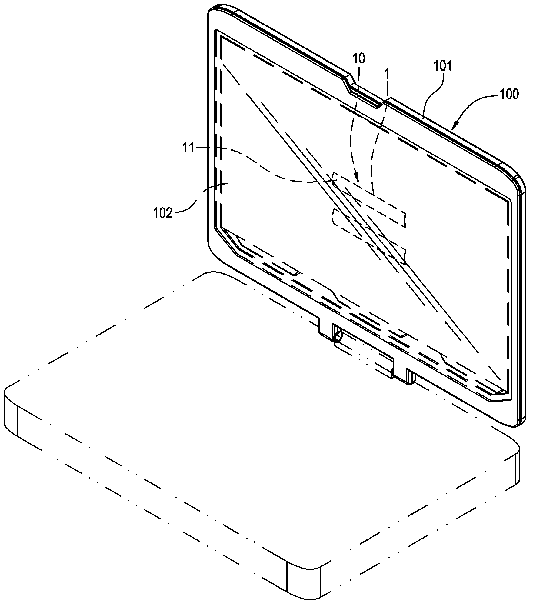
[0024] Please refer to figure 1 As shown, the combined schematic diagram of the first embodiment of the anti-compression structure of the present invention, the present invention provides a anti-compression structure of an electronic device. The electronic device 100 has a casing 101 and an electronic component 102 accommodated in the casing 101 . The compression structure 10 mainly includes a buffer body 1 .

[0025] Wherein, the electronic component 102 in this embodiment is a panel, but it is not limited thereto, and the electronic component 102 can be any component with an electronic circuit depending on the actual situation.

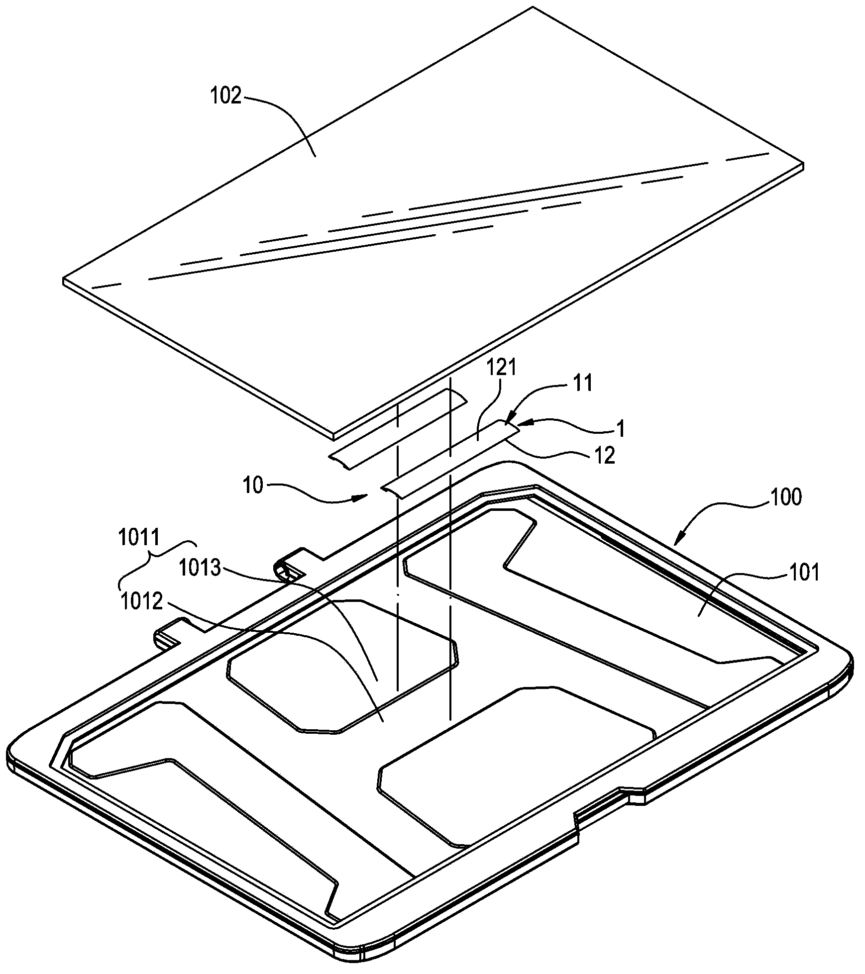
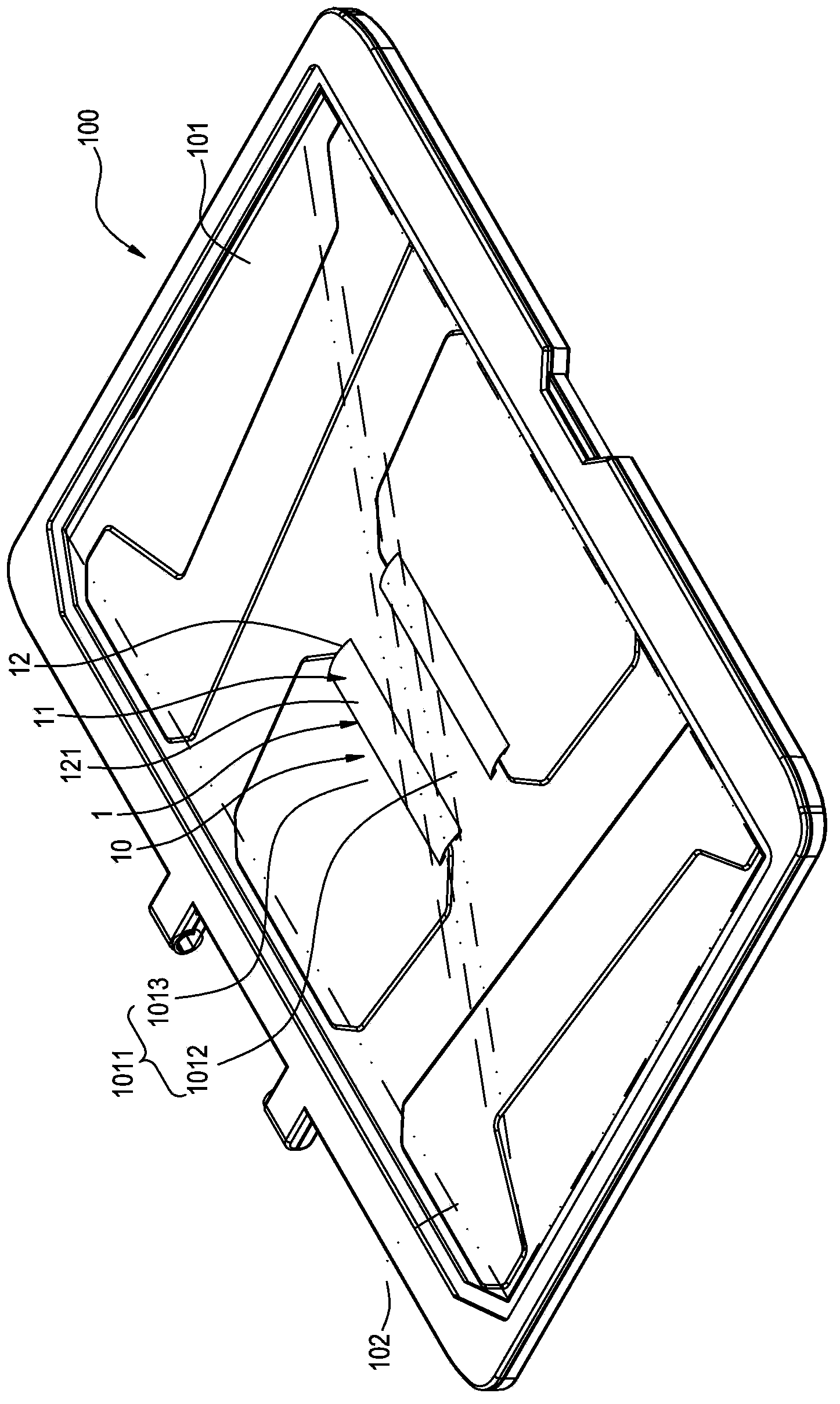
[0026] Please refer to figure 2 As shown, the three-dimensional exploded view of the first embodiment of the pressure-resistant structure of the present invention, wherein the casing 101 forms a protrusion 1011 toward the direction of the electronic component 102 . The protruding portion 1011 has a first step 1012 and a second step 1013 higher t...


PUM


Abstract

The invention provides a pressure-resistance structure of an electronic device. The electronic device is provided with a case and an electronic assembly contained in the case, a protrusion portion is formed on the case in the direction facing the electronic assembly, the pressure-resistance structure comprises a buffer body, the buffer body is fixed to the protrusion portion or the periphery of the protrusion portion, the buffer body is provided with at least one deformable convex face arranged in the direction of the electronic assembly, when the case is under pressure and the protrusion portion approaches the electronic assembly, and the deformable convex face makes contact with the electronic assembly and deforms so as to perform a pressure sharing function. Accordingly, when the protrusion portion approaches the electronic assembly, the deformable convex face will make contact with the electronic assembly first and deforms so as to provide a pressure sharing function, and then the situation that stress concentration occurs in the local position of the electronic assembly is avoided.

Description

【Technical field】 [0001] The invention relates to a pressure-resistant appliance for an electronic device, in particular to a pressure-resistant structure of the electronic device. 【Background technique】 [0002] All kinds of electronic products have a casing to protect the electronic components operating inside. But as consumers pay more and more attention to the beauty of the appearance of electronic products. Therefore, the casing has a shape design that can highlight the characteristics and brand recognition of electronic products. [0003] For example, the appearance of a rugged notebook computer is based on overall robustness and brand recognition. The casing will be designed with ups and downs grooves or channel-like designs to increase the strength and rigidity of the casing, or to provide a strong visual perception of the product. [0004] However, the undulating groove or channel-like design on the casing will produce a protrusion inside the casing. The protrud...

Claims


Application Information

Patent Timeline
Patent Type & Authority Applications(China)
IPC IPC(8): H05K5/02H05K7/00
Inventor 李国骧
Owner SHENXUN COMP KUNSHAN
Why Eureka
Try Eureka