Patterned cp test setup for cmos image sensor products
An image sensor and testing device technology, applied in the field of patterned CP testing devices, can solve problems such as low accuracy and low testing efficiency, and achieve the effect of improving efficiency
- Summary
- Abstract
- Description
- Claims
- Application Information
AI Technical Summary
Problems solved by technology
Method used
Image

Examples
Embodiment Construction
[0013] The embodiments of the present invention will be further described in detail below.
[0014] The band pattern CP testing device of CMOS image sensor product of the present invention, its preferred embodiment is:
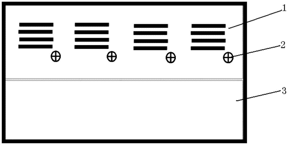
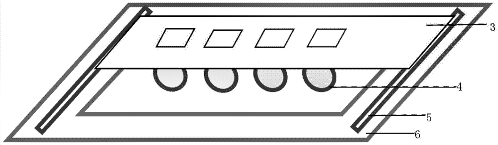
[0015] It includes a probe card, on which a pattern glass is installed, and a test pattern and an alignment mark are arranged on the pattern glass.
[0016] Both sides of the probe card are respectively provided with moving card slots, and a driving device is arranged in the moving card slots, and the graphic glass is installed on the driving device.
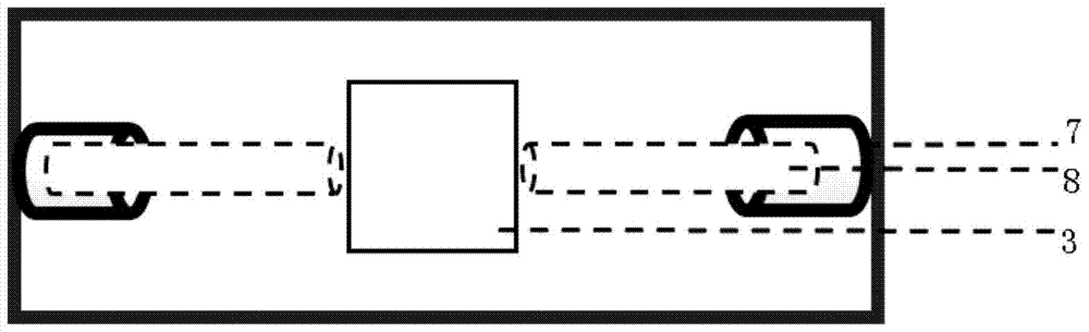
[0017] The driving device includes a stepping motor, the axis of the stepping motor is connected with a guide rail, and the graphic glass is arranged on the guide rail.
[0018] Both ends of the moving card slot are respectively provided with stepping motors, the shafts of the two stepping motors are arranged oppositely, and the guide rail is connected between the shafts of the two stepping motors.
[0019] Th...
PUM
 Abstract
Description
Claims
Application Information
 - R&D
- Intellectual Property
- Life Sciences
- Materials
- Tech Scout
- Unparalleled Data Quality
- Higher Quality Content
- 60% Fewer Hallucinations
Browse by: Latest US Patents, China's latest patents, Technical Efficacy Thesaurus, Application Domain, Technology Topic, Popular Technical Reports.
© 2025 PatSnap. All rights reserved.Legal|Privacy policy|Modern Slavery Act Transparency Statement|Sitemap|About US| Contact US: help@patsnap.com