Pixel structure, array substrate, display panel, display device and driving method for display device

A technology of pixel structure and display device, applied in static indicators, instruments, semiconductor devices, etc., can solve problems such as poor flickering of horizontal stripes, and achieve the effect of improving display effect, avoiding problems of horizontal stripes or poor flickering, and low power consumption

Active Publication Date: 2015-01-28
SHANGHAI AVIC OPTOELECTRONICS +1
View PDF7 Cites 18 Cited by
  • Summary
  • Abstract
  • Description
  • Claims
  • Application Information

AI Technical Summary

Problems solved by technology

[0006] In view of this, an embodiment of the present invention provides a pixel structure, an array substrate, a display panel, a display device, and a driving method thereof, so as to solve the pixel structure in which column inversion is used to achieve point inversion in the prior art. When there is a problem with the bit, there will be technical problems such as horizontal stripes or bad flickering

Method used


Image

  • Pixel structure, array substrate, display panel, display device and driving method for display device
  • Pixel structure, array substrate, display panel, display device and driving method for display device
  • Pixel structure, array substrate, display panel, display device and driving method for display device

Examples


Embodiment Construction

[0039] The present invention will be further described in detail below in conjunction with the accompanying drawings and embodiments. It should be understood that the specific embodiments described here are only used to explain the present invention, but not to limit the present invention. In addition, it should be noted that, for the convenience of description, only parts related to the present invention are shown in the drawings but not all content.

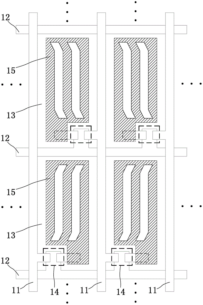
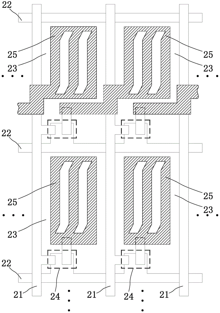
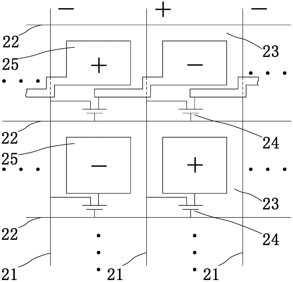
[0040] An embodiment of the present invention provides a pixel structure. Figure 2a It is a structural schematic diagram of a pixel structure provided by an embodiment of the present invention. like Figure 2aAs shown, the pixel structure includes: a plurality of data lines 21 and a plurality of scan lines 22; a plurality of pixel units 23 formed by intersections of the plurality of data lines 21 and the plurality of scan lines 22, wherein the pixel The unit 23 corresponds to a data line 21 and a scan line 22; a pixel elect...


PUM


Abstract

The invention discloses a pixel structure, an array substrate, a display panel, a display device and a driving method for the display device. According to the pixel structure, for any two adjacent rows of pixel units, a thin film transistor in one pixel unit in one row is electrically connected with a pixel electrode in a pixel unit which is positioned in the same row and is adjacent to the first side of the pixel unit, and a thin film transistor in a pixel unit in the other row is electrically connected with a pixel electrode in the same pixel unit or electrically connected with a pixel electrode in the pixel unit which is positioned in the same row and is adjacent to the second side of the pixel unit; the second side is opposite to the first side. According to the technical scheme, dot inversion is realized through row inversion or two-dot inversion is realized through two-row inversion to ensure low power consumption of polarity inversion; moreover, horizontal stripes or poor twinkle due to incomplete compensation of a common electrode on the voltage of the pixel electrodes in odd and even rows can be avoided, so that the display effect of the pixel structure can be improved.

Description

technical field [0001] The present invention relates to the field of display technology, in particular to a pixel structure, an array substrate, a display panel, a display device and a driving method thereof. Background technique [0002] With the development of display technology, liquid crystal display devices are more and more widely used, and the display effect is continuously improved. [0003] Generally speaking, in a liquid crystal display device, the polarity of the voltage difference applied to the liquid crystal molecules must be reversed at regular intervals to avoid permanent damage to the liquid crystal material due to polarization, and also to avoid Image persistence effect. Some common polarity inversion methods include: frame inversion (Frame Inversion), point inversion (Dot Inversion), row inversion (Column Inversion), column inversion (Row Inversion), two-column inversion and two-dot inversion Turn and wait. Among the above inversion methods, the power c...

Claims


Application Information

Patent Timeline
Patent Type & Authority Applications(China)
IPC IPC(8): G02F1/1362G02F1/1368G02F1/133H01L27/12
CPCG02F1/13306G02F1/136286G02F1/1368H01L27/1214G09G3/3614G09G2300/0426G09G2330/021G09G3/3648G09G2320/0247
Inventor 金慧俊曹兆铿简守甫林珧
Owner SHANGHAI AVIC OPTOELECTRONICS
Why Eureka
Try Eureka