Pixel circuit, driving method and display device

A pixel circuit and circuit technology, applied in static indicators, instruments, etc., can solve the problems of increasing the area of ​​a single pixel and reducing the PPI of the display device.

Active Publication Date: 2015-01-28
BOE TECH GRP CO LTD
View PDF6 Cites 24 Cited by
  • Summary
  • Abstract
  • Description
  • Claims
  • Application Information

AI Technical Summary

Problems solved by technology

However, setting a voltage compensation loop in each pixel circuit will lead to an increase in th

Method used


Image

  • Pixel circuit, driving method and display device
  • Pixel circuit, driving method and display device
  • Pixel circuit, driving method and display device

Examples


Embodiment 1

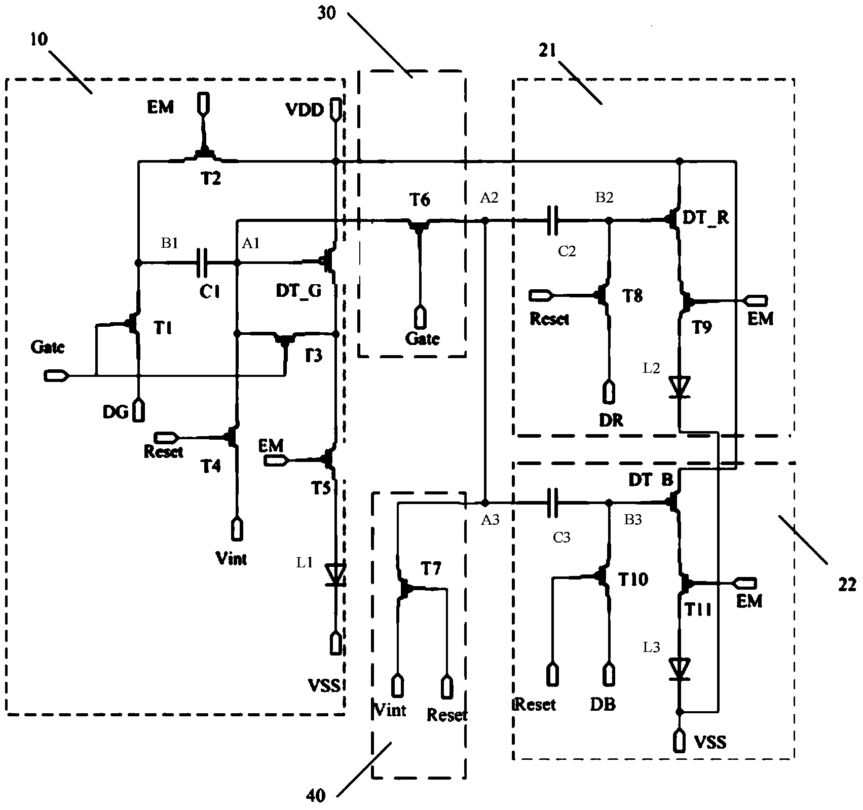
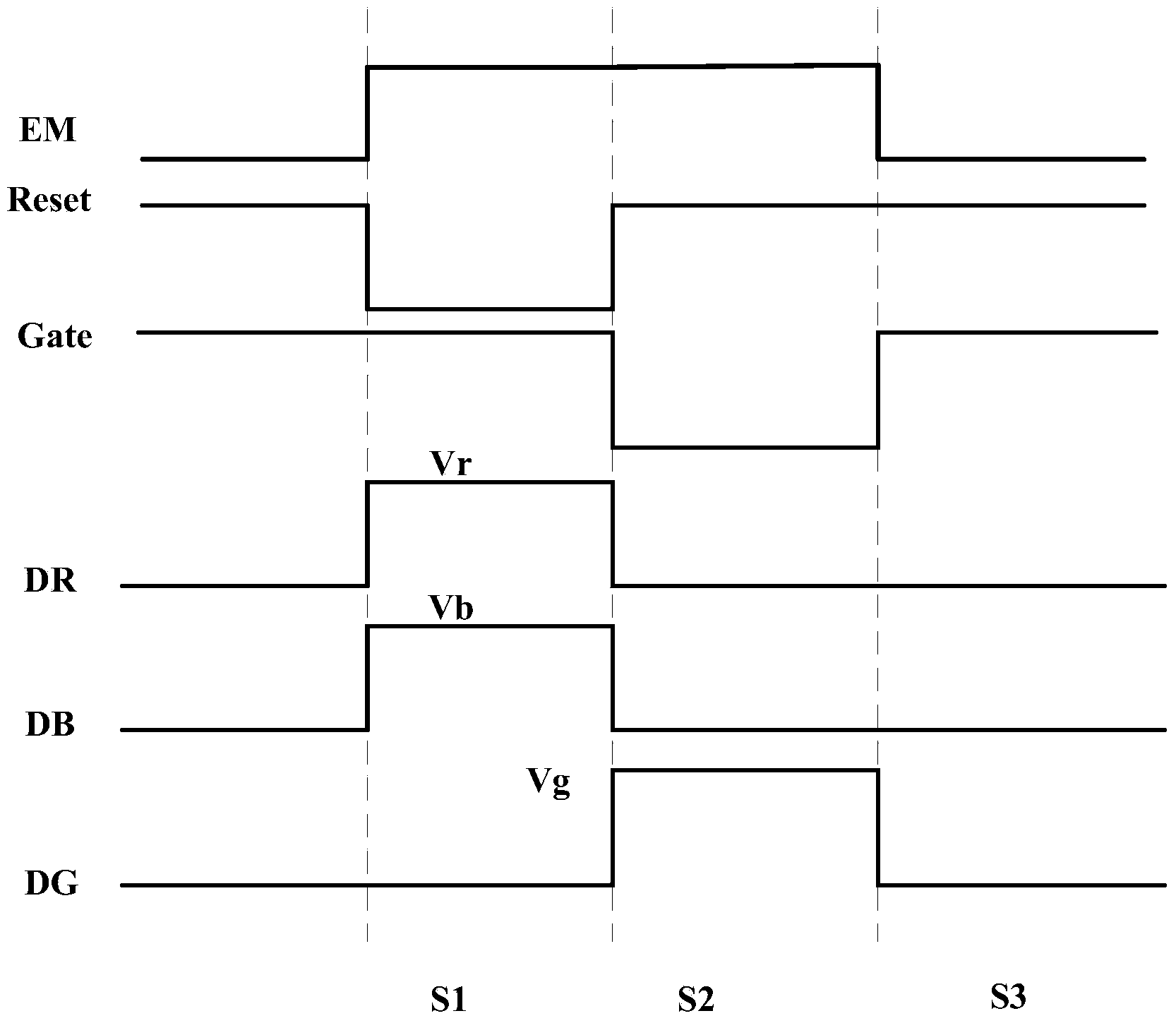
[0038] Embodiment 1 of the present invention provides a pixel circuit, such as figure 1As shown, the pixel circuit includes: a first sub-pixel circuit 10, two second sub-pixel circuits 21 and 22, a compensation sharing circuit 30, and a sharing control circuit 40, wherein the first sub-pixel circuit 10 includes 6 transistors, and the second A switching transistor T1, a second switching transistor T2, a third switching transistor T3, a fourth switching transistor T4, a fifth switching transistor T5, a first driving transistor DT_G, a first capacitor C1, and a first electroluminescent element L1 , the second sub-pixel circuit 21 includes three transistors, the eighth switch transistor T8, the ninth switch transistor T9 and the second drive transistor DT_R, a second capacitor C2 and a second electroluminescent element L2, the third sub-pixel circuit 22 Including three transistors, the tenth switching transistor T10, the eleventh switching transistor T11 and the third driving tran...

Embodiment 2

[0061] Such as Figure 4 Shown is a schematic structural diagram of the pixel circuit provided by Embodiment 2 of the present invention, and figure 1 the difference is, Figure 4 In the circuit, the gate of the first switch transistor T1 is connected to a signal output terminal Scan alone, and Figure 4 The circuit shown does not include the second switching transistor T2. At this time, the timing diagram of each signal driving the pixel circuit is as follows Figure 5 shown, with figure 2 The difference is that in the second stage, when a low-level signal is applied to Gate, a low-level signal is applied to Scan at the same time, the first switching transistor T1 is turned on, and the first voltage Vg1 is applied to DG, which will The voltage at the B1 terminal is set to Vg1; in the third stage, only a low-level signal is applied to Scan, the first switching transistor T1 is turned on, and other transistors are turned off, and the second voltage Vg2 is applied to DG to ma...

Embodiment 3

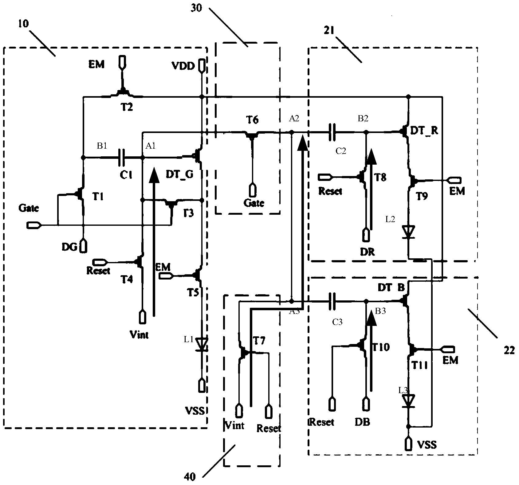
[0065] The schematic structural diagram of the pixel circuit provided by Embodiment 3 of the present invention is as follows Figure 6 shown, with Figure 4 The circuit provided is different in that the A1 terminal of the first capacitor C1 is connected to the B2 terminal of the second capacitor C2 and the B3 terminal of the third capacitor C3 through the sixth switching transistor T6, and at this time, the eighth switching transistor T8 is connected to the second capacitor The A terminal of C2, the tenth switching transistor T10 is connected to the A terminal of the third capacitor C3, and the seventh switching transistor T7 may not be provided at this time, and the driving method of the pixel circuit can be as follows Figure 7 shown, with Figure 5 The difference in the driving method is that in the second stage when the compensation of the second capacitor C2 and the third capacitor C3 is VDD+Vth1, the first voltage Vr1 and Vb1 are respectively applied to DR and DB, so th...


PUM


Abstract

The invention provides a pixel circuit, a driving method and a display device. The pixel circuit comprises multiple sub-pixel circuits, wherein a threshold value compensation module is arranged inside one sub-pixel circuit, and voltage compensated for through the threshold value compensation module is shared in the other sub-pixel circuits through a compensation sharing circuit. Because in the actual application, pixel circuits which are close are approximate in aging degree, a threshold value compensated for through the threshold value compensation module of one sub-pixel circuit can be used for threshold compensation on the other sub-pixel circuits. Because just one threshold value compensation module needs to be arranged for multiple pixels, the average area occupied by each pixel is decreased, and the PPI of the display device is conveniently improved.

Description

technical field [0001] The present invention relates to the field of display technology, in particular to a pixel circuit, a driving method and a display device. Background technique [0002] Organic light-emitting display (OLED) is one of the hot spots in the field of flat panel display research. Compared with liquid crystal display, OLED has the advantages of low energy consumption, low production cost, self-illumination, wide viewing angle and fast response speed. At present, OLEDs have begun to replace traditional liquid crystal (LCD) displays in display fields such as mobile phones, PDAs, and digital cameras. Pixel drive circuit design is the core technical content of OLED display, which has important research significance. [0003] Unlike TFT (Thin Film Field Effect Transistor)-LCD, which uses a stable voltage to control brightness, OLED is current-driven and requires a stable current to control light emission. [0004] Due to the process and device aging, in the ori...

Claims


Application Information

Patent Timeline
IPC IPC(8): G09G3/32G09G3/3208
CPCG09G3/3233G09G2300/0452G09G2300/0465G09G2300/0819G09G2300/0842G09G2300/0861G09G2320/0233G09G2300/043G09G2320/045G09G3/3291G09G3/2074G09G3/3258G09G2300/0809
Inventor 孙拓
Owner BOE TECH GRP CO LTD
Why Eureka
Try Eureka