TDC (time/digital conversion) method and device based on FPGA (field programmable gate array) fine delay unit
A technology of time-to-digital conversion and delay unit, which is applied in the direction of analog/digital conversion, code conversion, electrical components, etc., and can solve problems such as high cost, low scalability, and uniformity of restricted delay taps
- Summary
- Abstract
- Description
- Claims
- Application Information
AI Technical Summary
Problems solved by technology
Method used
Image
Examples
Embodiment Construction
[0016] Embodiments of the present invention will be described in detail below in conjunction with the accompanying drawings.
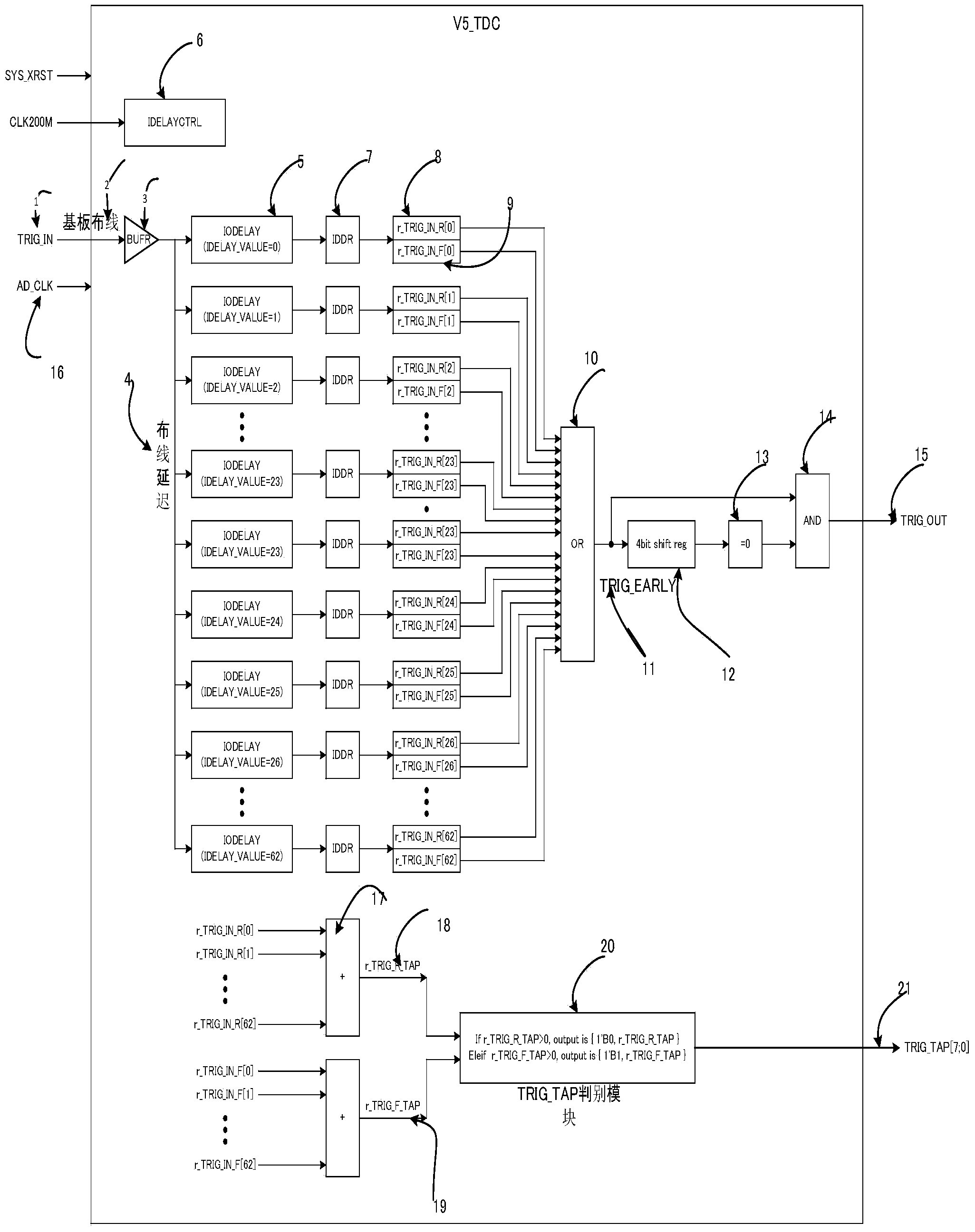
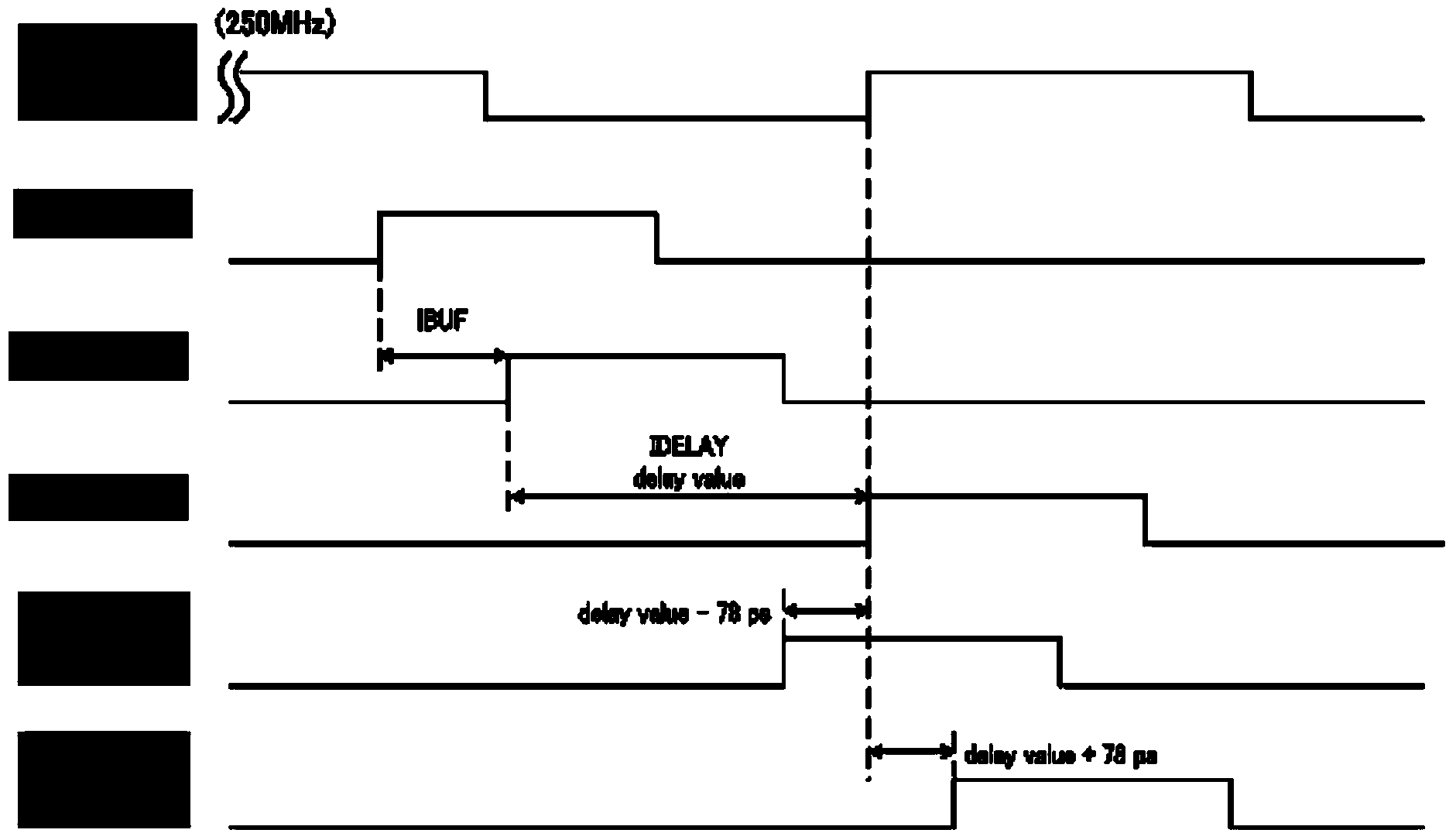
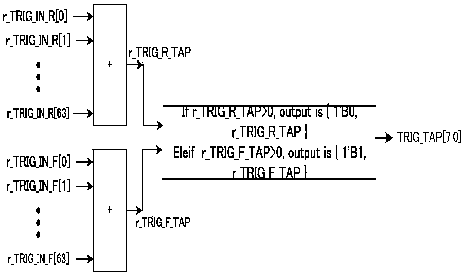
[0017] The internal structure is designed based on the TDC algorithm of the FPGA fine delay unit, which includes the following modules: 64-level fine delay unit IODELAY module (5), delay calibration unit IDELAYCTRL module (6), AD clock double-edge sampling output module IDDR (7) , the rising edge latch register r_TRIG_IN_R (8), the falling edge latch register r_TRIG_IN_F (9), the sampling value accumulation module (17). like figure 1 shown. The trigger signal TRIG_IN(1) of the optical path in the laser passes through the buffer BUFR(3) to improve the driving capability of the trigger signal. The trigger signal after BUFR passes through 64 equidistant wirings and reaches the 64 IODELAY modules at the same time. The delay of the 64 IODELAYs increases by 1 tap in turn, and the 64 IODELAYs sequentially increase by 1 tap to align with the rising edge of t...
PUM
 Abstract
Description
Claims
Application Information


