Display panel and display device

A technology for display panels and substrates, applied in nonlinear optics, instruments, optics, etc., can solve the problems that pixel electrodes cannot be displayed normally, display panel pressing and display unevenly, etc., to improve display effect, avoid uneven display, and not easily deformed Effect

Active Publication Date: 2015-03-25
XIAMEN TIANMA MICRO ELECTRONICS +1
View PDF5 Cites 12 Cited by
  • Summary
  • Abstract
  • Description
  • Claims
  • Application Information

AI Technical Summary

Problems solved by technology

[0005] The object of the present invention is to provide a display panel and a display device to solve the problem that when the existing display panel is working, a dark area appears in the edge area of ​​the pixel electrode due to abnormal display, and when the viewing surface is pressed with a finger, etc. , there will also be a dark area in this part, resulting in uneven display of the entire display panel.

Method used


Image

  • Display panel and display device
  • Display panel and display device
  • Display panel and display device

Examples


Embodiment 1

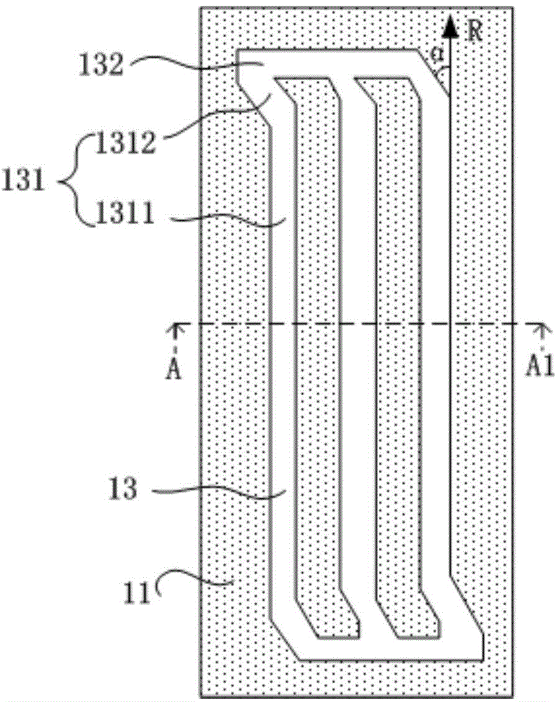
[0029] An embodiment of the present invention provides a display panel, the display panel adopts IPS or FFS drive mode, such as figure 2 and image 3 as shown, figure 2 It is a top view of the display panel provided by Embodiment 1 of the present invention, the display panel includes a first substrate (not shown in the figure), a second substrate (not shown in the figure) opposite to the first substrate, and a second substrate (not shown in the figure) A liquid crystal layer (not shown) between the first substrate and the second substrate, the liquid crystal layer is composed of liquid crystal molecules with a negative dielectric constant anisotropy, the pixel electrode 13 and the common electrode that are located on the first substrate and are insulated from each other 11. The alignment layer 17 covering the pixel electrode 13 and the common electrode 11, the alignment layer 17 has a preset alignment direction R, wherein the pixel electrode 13 includes at least two branch ...

Embodiment 2

[0046] Such as Figure 9 Shown is a schematic structural diagram of a pixel electrode according to Embodiment 2 of the present invention. The display panel adopts the second-generation FFS technology (Ultra FFS), and the pixel electrode is a bent strip electrode with a double-domain structure.

[0047] Specifically, the display panel includes:

[0048] The first substrate, the second substrate opposite to the first substrate, and the liquid crystal layer arranged between the first substrate and the second substrate, the liquid crystal layer is composed of liquid crystal molecules with negative dielectric constant anisotropy, and is located on the second substrate. A pixel electrode 23 and a common electrode 21 that are insulated from each other on a substrate cover an alignment layer (not shown in the figure) of the pixel electrode 23 and the common electrode 21, and the alignment layer has a preset alignment direction R, wherein the pixel electrode 23 includes The first pixe...

Embodiment 3

[0052] Such as Figure 10 Shown is a schematic structural diagram of a pixel electrode according to Embodiment 3 of the present invention, and the pixel electrode is a bent strip electrode.

[0053] Specifically, the display panel includes:

[0054] The first substrate, the second substrate opposite to the first substrate, and the liquid crystal layer arranged between the first substrate and the second substrate, the liquid crystal layer is composed of liquid crystal molecules with negative dielectric constant anisotropy, and is located on the second substrate. A pixel electrode 33 and a common electrode 31 that are insulated from each other on a substrate cover an alignment layer (not shown in the figure) of the pixel electrode 33 and the common electrode 31, and the alignment layer has a preset alignment direction R, wherein the pixel electrode 33 includes The branch electrode 331 and the end electrode 332 connected to the end of the branch electrode 331, the branch electro...


PUM


Abstract

The invention discloses a display panel and a display device. The display panel comprises a first substrate, a second substrate opposite to the first substrate, a liquid crystal layer arranged between the first substrate and the second substrate, a pixel electrode, a public electrode and an alignment layer. The liquid crystal layer is composed of liquid crystal molecules with dielectric constant anisotropy being negative, the pixel electrode and the public electrode are located on the first substrate and insulated from each other, the alignment layer covers the pixel electrode and the public electrode and has a preset alignment direction, the pixel electrode comprises at least two branch electrodes and an end electrode connecting the ends of the branch electrodes, each branch electrode comprises a body portion and a bend connection portion, each bend connection portion is connected between the corresponding body portion and the end electrode, and a first angle formed between each bend connection portion and the alignment direction is larger than or equal to 5 degrees and smaller than or equal to 25 degrees. The display panel and the display device can solve the phenomenon that pressing display of the display panel is not uniform, the penetration rate is increased along with reducing of a bend angle, drive voltage is lowered, and therefore power consumption is lowered.

Description

technical field [0001] The present invention relates to the field of display technology, in particular to a display panel and a display device including the display panel. Background technique [0002] Liquid Crystal Display (LCD) is a display made of liquid crystal material, which has the characteristics of light and thin, low power consumption and large amount of displayed information. An LCD generally includes a liquid crystal display panel for displaying pictures and a circuit part for supplying signals to the liquid crystal display panel. The liquid crystal display device generally includes a first substrate and a second substrate, which are bonded to each other by a sealant and separated by a gap, and liquid crystal material is filled in the gap between the first substrate and the second substrate. [0003] The widely used liquid crystal display modes include twisted nematic mode (Twist Nematics, TN), vertical alignment mode (Vertical Alignment, VA), in-plane flipping...

Claims


Application Information

Patent Timeline
Patent Type & Authority Applications(China)
IPC IPC(8): G02F1/1343G02F1/1333
CPCG02F1/134309G02F1/134327
Inventor 吴玲凌安恺沈柏平
Owner XIAMEN TIANMA MICRO ELECTRONICS
Why Eureka
Try Eureka