Eureka AIR delivers breakthrough ideas for toughest innovation challenges, trusted by R&D personnel around the world.

Alignment device for exposure of circuit board and alignment method for exposure of circuit board

An alignment device and circuit board technology, applied in the field of circuit board production, can solve problems such as increased production tooling costs, inability to align, and poor compatibility, so as to save labor costs and production costs, ensure product quality, and reduce production costs. Effect

Inactive Publication Date: 2015-03-25
ZHENJIANG HUAYIN PRINTED CIRCUIT BOARD
View PDF7 Cites 0 Cited by
  • Summary
  • Abstract
  • Description
  • Claims
  • Application Information

AI Technical Summary

Problems solved by technology

[0004] However, the above-mentioned alignment has the following disadvantages: 1. An exposure machine generally requires three people to operate, one of whom operates the exposure machine, and the other two perform alignment production. The work efficiency is low and the labor cost is high; 2. Poor compatibility of expansion and contraction: Once the product size changes too much, it cannot be aligned, and new tools can only be recompensated according to the size after expansion and contraction, which will cause production interruption and increase the cost of production tools

Method used


Image

  • Alignment device for exposure of circuit board and alignment method for exposure of circuit board
  • Alignment device for exposure of circuit board and alignment method for exposure of circuit board
  • Alignment device for exposure of circuit board and alignment method for exposure of circuit board

Examples


Embodiment Construction

[0018] In the following, the present invention will be further clarified with reference to the accompanying drawings and specific embodiments. It should be understood that these embodiments are only used to illustrate the present invention and not to limit the scope of the present invention. After reading the present invention, those skilled in the art will understand various aspects of the present invention. Modifications in equivalent forms fall within the scope defined by the appended claims of this application.

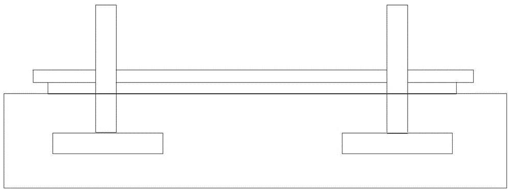
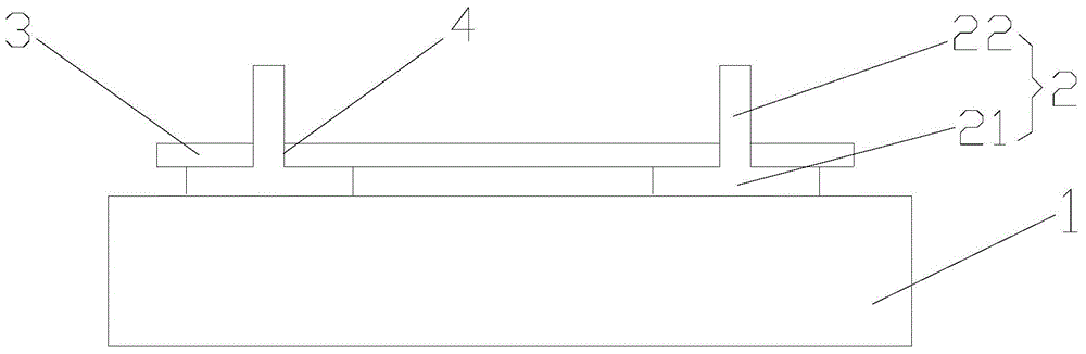
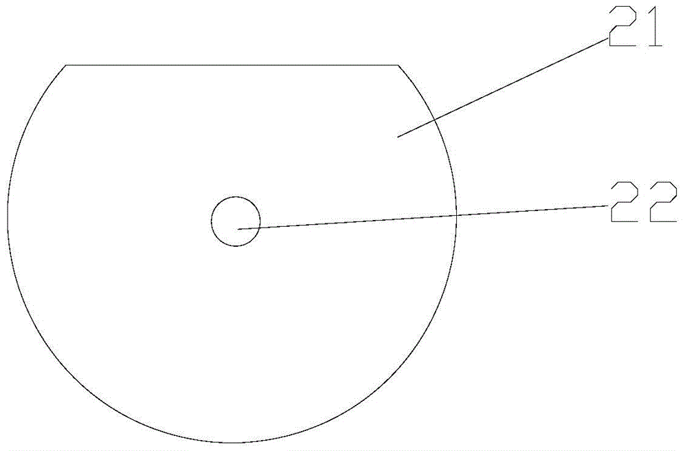
[0019] Such as figure 2 As shown, a circuit board exposure and alignment device includes an exposure table 1, a pin 2, and a film 3. The pin 2 is composed of a bottom plate 21 and a column 22, wherein the column 22 directly extends from the bottom plate 21. Several sets of through holes 4 with a diameter equivalent to the diameter of the cylinder 22 are provided on both sides of the film 3, and the cylinder 22 of the pin 2 is sleeved in the through hole 4 of the film...


PUM


Abstract

The invention discloses an alignment device for exposure of a circuit board and an alignment method for the exposure of the circuit board. The alignment device for the exposure of the circuit board comprises an exposure table top, pins and a film, wherein each pin comprises a bottom plate and a cylinder which extends out of the bottom plate; the bottom plate is positioned between the exposure table top and the film; the film is arranged on the cylinders in a sleeving manner through a plurality of groups of through holes formed in the two sides of the film. The alignment method for the exposure of the circuit board comprises the following steps: cutting a copper foil into a required shape; drilling a plurality of alignment holes in the edge of the copper foil; arranging the cylinders of the pins into the through holes of the film from bottom to top in the sleeving manner; placing the bottom plates of the pins on the exposure table top to form the alignment device; arranging the alignment holes of the copper foil on the cylinders of the pins in the sleeving manner, and aligning the copper foil with the film. The alignment device and the alignment method have the advantages that manpower cost and production cost are greatly reduced; the problems of loss, accuracy reduction and the like caused by friction between the film and other components or equipment are avoided; the product quality is guaranteed.

Description

Technical field [0001] The invention relates to the field of circuit board production, in particular to a circuit board exposure and alignment device and an alignment method thereof. Background technique [0002] With the development of science and technology, ultra-thin and ultra-light portable electronic products have become the trend and direction of development. Correspondingly, the circuit boards using these products are getting smaller and smaller, requiring higher and higher alignment accuracy. For example, FPC flexible circuit boards have finer circuits and dense pads, especially FPCs in the fields of digital cameras and cameras. Therefore, in circuit board processing engineering, accurate product processing and accurate alignment of circuits are particularly important. In general FPC, the relative fitting tolerance of product lines in the industry is sometimes as high as ±0.05mm, which requires high alignment. [0003] Pin positioning is a common exposure method in the c...

Claims


Application Information

Patent Timeline
Patent Type & Authority Applications(China)
IPC IPC(8): G03F9/00
Inventor 赵建梁
Owner ZHENJIANG HUAYIN PRINTED CIRCUIT BOARD
Why Eureka
Eureka Blog
Learn More