Electronic component recognizing method and system

A technology of electronic components and identification methods, applied in the electronic field, can solve problems such as high difficulty, many quality problems, difficult assembly positions, etc., and achieve the effects of low cost, fast and accurate identification, high degree of automation and reliability

Inactive Publication Date: 2015-03-25
GUANGZHOU SHIYUAN ELECTRONICS CO LTD
View PDF3 Cites 30 Cited by
  • Summary
  • Abstract
  • Description
  • Claims
  • Application Information

AI Technical Summary

Problems solved by technology

[0004] Because the circuit board components and electronic circuits are very different, and the distribution of various electronic components is different, it is very difficult to find the corresponding electronic component assembly position in the circuit board distribution of various electronic components, which is time-consuming and laborious. And manual inspection high error rate
With the rapid development of microelectronics technolog

Method used


Image

  • Electronic component recognizing method and system
  • Electronic component recognizing method and system
  • Electronic component recognizing method and system

Examples


Embodiment Construction

[0052] The following will clearly and completely describe the technical solutions in the embodiments of the present invention with reference to the drawings in the embodiments of the present invention.

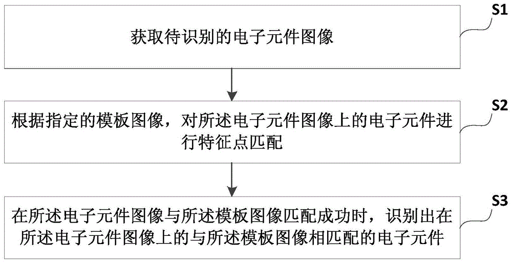
[0053] see figure 1 , is a flow chart of the steps of the electronic component identification method provided in the first embodiment of the present invention.

[0054] In this embodiment, the electronic component identification method specifically includes the following steps S1-S3:

[0055] Step S1: Obtain an image of the electronic component to be identified.

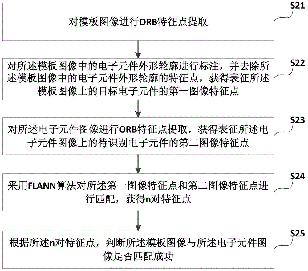
[0056] Step S2: Perform feature point matching on the electronic components on the electronic component image according to the specified template image.

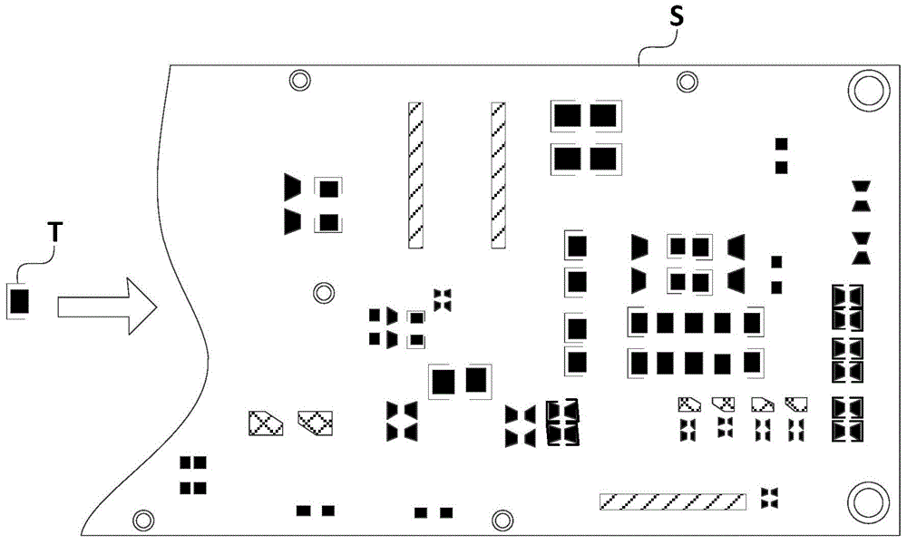
[0057] see figure 2 , is a schematic diagram of electronic component image matching provided by the first embodiment of the present invention.

[0058] Wherein, the template image T is the image of the target electronic component that needs to be identified in...


PUM


Abstract

The invention discloses an electronic component recognizing method. The method comprises the steps of acquiring an electronic component image to be recognized, conducting feature point matching on electronic components on the electronic component image according to a specific model image, and recognizing the electronic component matched with the model image on the electronic component image when the electronic component image is successfully matched with the model image. The invention further provides an electronic component recognizing system. By the adoption of the technical scheme, automatic electronic component recognition is achieved, and recognition rate and recognition reliability are improved.

Description

technical field [0001] The invention relates to the field of electronic technology, in particular to an electronic component identification method and system. Background technique [0002] All kinds of electronic products are composed of electronic circuits with different functions printed on circuit boards, and the basic units that form electronic circuits are various electronic components (referred to as electronic components or electronic devices). During the production process of the circuit board, many electronic devices need to be packaged, and in the packaging process, the installation of other components is often affected by the wrong electronic devices. [0003] At present, the assembly process of electronic components on printed boards is mainly assembled according to the assembly drawing and list of electronic components in the work guidance documents such as process regulations. Especially in the printed board production line of small batches of electronic produ...

Claims


Application Information

Patent Timeline
IPC IPC(8): G06K9/46
CPCG06V10/443
Inventor 廖明熙
Owner GUANGZHOU SHIYUAN ELECTRONICS CO LTD
Why Eureka
Try Eureka