Terahertz light source chip and manufacturing method thereof, terahertz light source device and manufacturing method thereof, and terahertz light source module and manufacturing method thereof

A terahertz and light source technology, applied in semiconductor devices, solid-state lasers, electrical components, etc., can solve problems such as large loss, unfavorable conversion efficiency, and low quality factor

Active Publication Date: 2015-03-25
SUZHOU INST OF NANO TECH & NANO BIONICS CHINESE ACEDEMY OF SCI
View PDF9 Cites 50 Cited by
  • Summary
  • Abstract
  • Description
  • Claims
  • Application Information

AI Technical Summary

Problems solved by technology

Due to the limited electron mobility, the plasmonic wave mode has low quality factor and high loss, which is not conducive to the improvement of conversion efficiency from driving current to plasmonic wave excitation
[0012] In the above-mentioned existing technology based on plasma waves to realize terahertz emission sources, there is no clear solution to problems such as the low quality factor of plasma waves

Method used


Image

  • Terahertz light source chip and manufacturing method thereof, terahertz light source device and manufacturing method thereof, and terahertz light source module and manufacturing method thereof
  • Terahertz light source chip and manufacturing method thereof, terahertz light source device and manufacturing method thereof, and terahertz light source module and manufacturing method thereof
  • Terahertz light source chip and manufacturing method thereof, terahertz light source device and manufacturing method thereof, and terahertz light source module and manufacturing method thereof

Examples


Embodiment approach 1

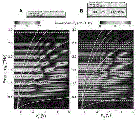
[0147] This embodiment provides a terahertz light source chip (also referred to as a first terahertz light source chip in this embodiment), a corresponding light source device and assembly, and a manufacturing method thereof. figure 1 It is a schematic diagram of the principle of the terahertz light source chip according to this embodiment. figure 2 It is the dispersion relation diagram of the plasma wave and the dispersion relation diagram of the cavity mode of the terahertz resonant cavity. Figure 3A It is a top view of the structure of the terahertz light source of this embodiment, Figure 3B for Figure 3A The cross-sectional view of the terahertz light source chip and the schematic diagram of the current drive.

[0148] like figure 1 As shown, the terahertz light source chip includes: a two-dimensional electron gas mesa 1; an electrode (not shown) for exciting a plasma wave 6 formed on the two-dimensional electron gas mesa 1; a terahertz resonant cavity 3, the The t...

Embodiment approach 2

[0214] This embodiment is further improved on the basis of Embodiment 1, and another chip (also referred to as a second terahertz light source chip in this embodiment), corresponding light source devices and components, and its manufacturing method are provided to provide The escape loss of terahertz light is reduced, thereby further improving the quality factor of the terahertz resonant cavity, enhancing the coupling strength between the cavity mode of the resonant cavity and the plasma wave mode, and improving the conversion efficiency.

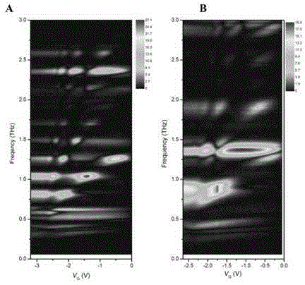
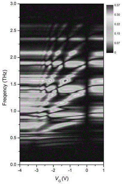
[0215] Image 6 It is a schematic structural diagram of the terahertz light source chip in this embodiment. Figure 7 To show one form of the plasmon wave mode and the terahertz resonator mode generated under the grating-resonator coupling.

[0216] Such as Image 6 As shown, the terahertz light source chip of this embodiment includes: a two-dimensional electron gas mesa 1; electrodes (such as source S and drain D; source and drain electr...


PUM


Abstract

The invention provides a terahertz light source chip and a manufacturing method thereof, a terahertz light source device and a manufacturing method thereof, and a terahertz light source module and a manufacturing method thereof. The light source chip comprises a two-dimensional electron gas mesa, an electrode, a terahertz resonant cavity and an optical grating, wherein the electrode is formed on the two-dimensional electron gas mesa and used for exciting plasma waves; the terahertz resonant cavity is formed below the two-dimensional electron gas mesa, and a holophote is arranged on the bottom surface of the resonant cavity; the optical grating is formed on the two-dimensional electron gas mesa and used for coupling a plasma wave mode to a terahertz resonant cavity mode so that terahertz wave emission can be generated. Plasma polaritons are formed by strongly coupling the terahertz resonant cavity mode to the plasma wave mode in two-dimensional electron gas under the optical grating, terahertz wave emission can be generated through electric excitation of the plasma polaritons, the problem that terahertz emission is low in frequency or working temperature because of high frequency oscillation relaying on a single electron or quantum jump relaying on a single electron is solved, and the emission frequency range and the working temperature range are widened.

Description

technical field [0001] The present invention relates to a technology for generating terahertz radiation, and more specifically, to a terahertz light source chip, a light source device, a light source component and a manufacturing method thereof. Background technique [0002] Terahertz wave (terahertz wave) refers to the frequency of 0.1-10THz (1THz=1000GHz=10 12 Hz), with a wavelength of 30 microns to 3 mm, between the millimeter wave band and the infrared light band of the electromagnetic spectrum, formerly known as submillimeter waves or far infrared. The radiation of terahertz waves is also called terahertz radiation. A device or device capable of generating terahertz wave radiation is called a terahertz source (terahertz source) or a terahertz emitter (terahertz emitter). [0003] The existing technical solutions for generating terahertz radiation can be mainly divided into the following three categories: [0004] The first category is electronic technology solutions,...

Claims


Application Information

Patent Timeline
Patent Type & Authority Applications(China)
IPC IPC(8): H01S1/02
CPCH01S1/02H01L29/42316H01L33/58H01L29/778H01L33/0041H01L33/0095H01L33/06H01L33/105H01L33/26H01L33/28H01L33/30H01L33/32H01L33/34H01L33/54
Inventor 秦华孙建东黄永丹郑中信吴东岷蔡勇张宝顺
Owner SUZHOU INST OF NANO TECH & NANO BIONICS CHINESE ACEDEMY OF SCI
Why Eureka
Try Eureka