Loudspeaker protection circuit
A technology for protecting circuits and speakers, applied to emergency protection circuit devices, transducer circuits, circuit devices, etc., can solve problems such as speaker burnout, and achieve the effect of preventing burnout and protecting speakers
- Summary
- Abstract
- Description
- Claims
- Application Information
AI Technical Summary
Problems solved by technology
Method used
Image

Examples
Embodiment 1
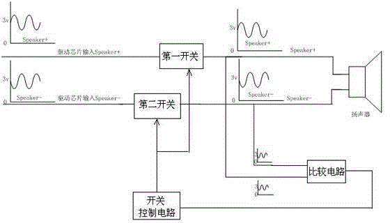
[0021] Embodiment 1, this embodiment proposes a loudspeaker protection circuit, such as figure 1 As shown, it includes a first switch and a second switch respectively connected to the two-way differential audio signal lines of the loudspeaker, and also includes a comparison circuit for comparing whether the two-way signals of the two-way differential audio signals are the same, and the same as the A switch control circuit connected to the comparison circuit, the comparison circuit sends a comparison signal to the switch control circuit, and the switch control circuit generates a control signal for controlling the conduction states of the first switch and the second switch according to the comparison signal and sent to the first switch and the second switch. In the speaker protection circuit of the present invention, by setting the first switch and the second switch on the differential audio signal transmission line of the speaker, a control command for controlling the first sw...
Embodiment 2
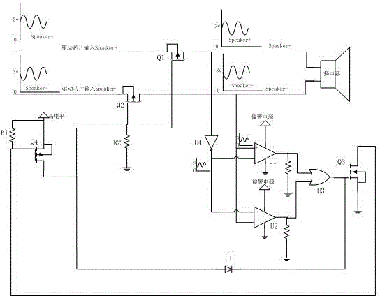
[0027] Embodiment 2. This embodiment presents a circuit schematic diagram of another embodiment of the switch control circuit in the speaker protection circuit. Other circuit parts of the speaker protection circuit are the same as those in Embodiment 1, and will not be repeated here. In this example, if image 3 As shown, the switch control circuit includes a third NPN transistor Q3 and a fourth PNP transistor Q4, the base of the third NPN transistor Q3 is connected to the output terminal of the OR circuit U3, and the third The emitter of the NPN transistor Q3 is connected to the ground, the collector of the third NPN transistor Q3 is connected to the base of the fourth PNP transistor Q4, and the collector of the fourth PNP transistor Q4 is connected to the DC One of the emitters of the fourth PNP transistor Q4 is connected to the gates of the first PMOS transistor Q1 and the second PMOS transistor Q2 respectively. The principle of the switch control circuit in this implement...
PUM
 Abstract
Description
Claims
Application Information
 - R&D
- Intellectual Property
- Life Sciences
- Materials
- Tech Scout
- Unparalleled Data Quality
- Higher Quality Content
- 60% Fewer Hallucinations
Browse by: Latest US Patents, China's latest patents, Technical Efficacy Thesaurus, Application Domain, Technology Topic, Popular Technical Reports.
© 2025 PatSnap. All rights reserved.Legal|Privacy policy|Modern Slavery Act Transparency Statement|Sitemap|About US| Contact US: help@patsnap.com