Interleaved switching power supply and control method thereof

A switching power supply, interleaved technology, applied in the field of interleaved parallel switching power supply and its control, can solve the problems of poor dynamic response, complicated compensation design, etc.

Active Publication Date: 2015-04-01
SILERGY SEMICON TECH (HANGZHOU) CO LTD
5 Cites 22 Cited by

AI-Extracted Technical Summary

Problems solved by technology

The out-of-phase control of the interleaved parallel switching power supply in the prior art usually adopts the fixed-frequency control method, such as using a fixed out-of-ph...

Abstract

The invention discloses an interleaved switching power supply and a control method thereof. The control method includes the following steps: an AC ripple signal is generated according to switching control signals of a plurality of power level circuits; the AC ripple signal is then superposed with an output voltage feedback signal; after a signal generated after the superposition is compared with a reference voltage signal, frequency division is carried out to obtain continuity signals of the power level circuits; certain phase angles exist among phases of the continuity signals after the frequency division, so that phase-staggered continuity of main switching tubes can be achieved. The interleaved switching power supply provided by the invention has the advantages of accurate phase stagger, rapid response and good effect.

Application Domain

Apparatus without intermediate ac conversion

Technology Topic

Phase anglePower level +3

Image

  • Interleaved switching power supply and control method thereof
  • Interleaved switching power supply and control method thereof
  • Interleaved switching power supply and control method thereof

Examples

  • Experimental program(1)

Example Embodiment

[0050] Several preferred embodiments of the present invention are described in detail below with reference to the accompanying drawings, but the present invention is not limited to these embodiments. The present invention covers any alternatives, modifications, equivalent methods and arrangements made within the spirit and scope of the present invention. In order to give the public a thorough understanding of the present invention, specific details are described in detail in the following preferred embodiments of the present invention, and those skilled in the art can fully understand the present invention without the description of these details.
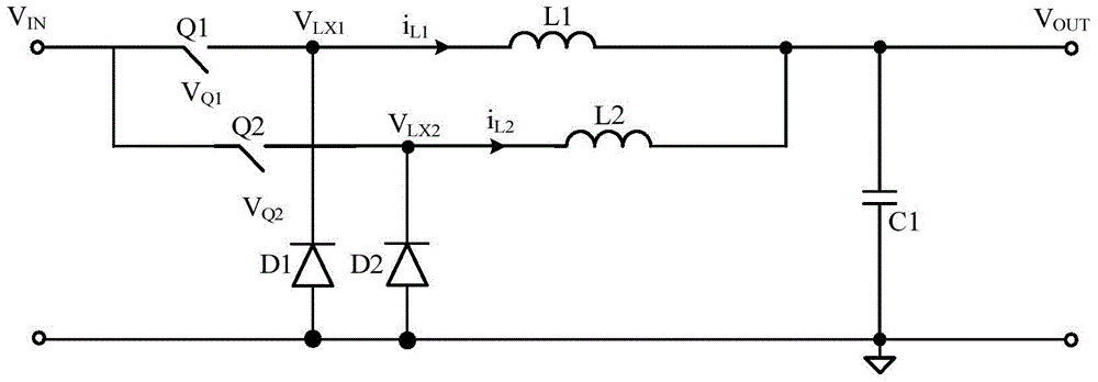
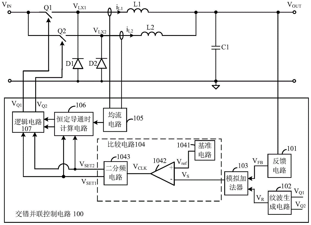
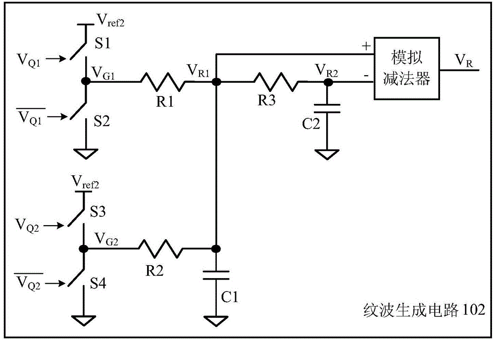
[0051] refer to figure 2Shown is a circuit block diagram of a parallel interleaved switching power supply according to the present invention. In the embodiment of the present invention, the parallel interleaved switching power supply includes two parallel step-down power stage circuits, but is not limited to this. The power supply includes a staggered parallel control circuit 100, and the staggered parallel control circuit 100 is used to generate multiple switch control signals to control the on and off of the main switch tubes in each power stage circuit, wherein the staggered parallel control circuit includes: A feedback circuit 101, a ripple generation circuit 102, an addition circuit 103 and a comparison circuit 104, the feedback circuit 101 receives the output voltage signal of the switching power supply to generate an output voltage feedback signal V FB; The ripple generation circuit 102 receives the switch control signal of the main switch tube in each power stage circuit, such as figure 2 V in Q1 , V Q2 , so as to generate an AC ripple signal V R , and, the AC ripple signal V R The frequency is a multiple of the switching frequency, and the multiple is consistent with the number of the power stage circuits. For example, in this embodiment, the number of the power stage circuits is 2, then the AC ripple signal V R The frequency is twice the switching frequency. It should be noted that, in this embodiment, the switching frequencies of each channel are the same; the summing circuit feeds the output voltage feedback signal V FB and the AC ripple signal V R added to generate the superimposed signal V S , the adding circuit here is an analog adder.
[0052] Then, the comparison circuit 104 receives the superimposed signal V S and the reference voltage signal V ref ,like figure 1 As shown, in this embodiment, the comparison circuit 104 specifically includes a reference circuit 1041, a comparator 1042 and a frequency dividing circuit 1043, and the reference circuit 1041 is used to generate the reference voltage signal V ref , the positive input terminal of the comparator 1042 receives the reference voltage signal V ref , the reverse input terminal receives the superimposed signal V S , after the comparison, the comparison signal V is generated CLK , the divide-by-two circuit 1043 receives the comparison signal V CLK After frequency division processing to generate two conduction signals V SET1 and V SET2 , the turn-on signal V SET1 and V SET2 They differ by a predetermined phase angle. In this embodiment, the two are 180° out of phase, and the turn-on signal V SET1 and V SET2 They are respectively used to control the conduction of the main switch tubes such as Q1 and Q2 in the power stage circuit, so that the phase-staggered conduction of the multi-channel main switch tubes is realized.
[0053] Further, in this embodiment, the interleaved parallel control circuit 100 further includes a current sharing circuit 105 , a constant on-time calculation circuit 106 and a logic circuit 107 , and the current sharing circuit 105 samples samples in the multi-channel power stage circuit. The inductor current signal is generated according to the current sharing signal; for example, in this embodiment, the current sharing circuit 105 compares the average value of the two inductor currents, and when the average value is not equal, increases or shortens the second main switch tube. After the on-time of the second channel is adjusted for many times, the average value of the currents of the two channels is finally made equal, and the current sharing circuit may be a suitable circuit structure in the prior art. The constant on-time calculation circuit 106 receives the current sharing signal and the multi-channel conduction signal to generate a multi-channel disconnection signal to control the disconnection of the multi-channel main switch tubes. For example, in this embodiment, the The constant on-time calculation circuit 106 is based on the above-mentioned on-signal V SET1 and V SET2 The trigger edge starts timing, and when it reaches the expected fixed time value, a disconnection signal is generated, or further, according to the above-mentioned turn-on signal V SET1 and V SET2 And the current sharing signal adjusts the on time of a certain channel, so that the disconnection signal is generated after a preset time value. The logic circuit 107 receives the multi-channel turn-on signal and the multi-channel disconnect signal, and outputs a multi-channel switch control signal such as V at the output end. Q1 and V Q2 In order to control the on-off of the multi-channel main switch, the logic circuit here may be a suitable circuit structure such as an RS flip-flop.
[0054] In the technical solution of the present invention, in order to realize accurate out-of-phase conduction according to the multi-channel switch tube, the AC ripple signal 102 in the present invention is generated according to the control signals of each channel, refer to image 3 shown as figure 2 A specific implementation of the ripple generation circuit; the ripple generation circuit 102 further includes a multi-channel chopper circuit, a first filter circuit, a second filter circuit and a subtraction circuit, where the multi-channel chopper circuit and The multi-channel power stage circuits are in one-to-one correspondence. In this embodiment, the multi-channel chopper circuit includes two chopper circuits, such as image 3 As shown, the first chopper circuit includes a chopper circuit composed of switches S1 and S2, and the input end of the first chopper circuit receives a voltage source V ref2 , the switch S1 is controlled by the switch control signal V corresponding to the main switch tube Q1 Q1 Control its switching action, switch S2 is controlled by the switch control signal V corresponding to the main switch tube Q1 Q1 The non-signal controls its switching action; the second chopper circuit includes a chopper circuit composed of switches S3 and S4, and the input end of the second chopper circuit receives the voltage source V ref2 , the switch S3 is controlled by the switch control signal V corresponding to the main switch tube Q2 Q2 Control its switching action, switch S4 is controlled by the switch control signal V corresponding to the main switch tube Q2 Q2 The non-signal controls its switching action. Voltage source V ref2 After being chopped by the first chopper circuit, a first chopper signal V is generated G1 , the first chopped signal V G1 with the voltage V of the LX1 point in the power stage circuit LX1 In the same phase; in the same way, the voltage source V ref2 After being chopped by the first chopper circuit, the voltage V generated at the LX2 point in the power stage circuit LX2 The second chopped signal V of the same phase G2.
[0055] Next, the first chopping signal V G1 and the second chopped signal V G2 After being filtered by the first filter circuit, a first filtered signal V in the same phase as the inductor current in the power stage circuit is generated R1; Here, the first filter circuit includes a plurality of resistors and a first capacitor, such as image 3 The resistor R1 and resistor R2 in the resistor R1, the first end of the resistor R1 is connected to the output end of the first chopper circuit to receive the first chopper signal V G1 , the first end of the resistor R2 is connected to the output end of the second chopper circuit to receive the second chopper signal V G2 , the second ends of the resistor R1 and the resistor R2 are both connected to the first end of the first capacitor C1; the second end of the first capacitor is grounded, and the voltage of the first end of the first capacitor is used as the first end of the first capacitor. A filtered signal V R1. Here, the first filtered signal is a triangular wave signal with the same phase as the inductor current.
[0056] After that, the first filtered signal V R1 After being filtered by the second filter circuit, a smoother second filtered signal V is generated R2; Here, the second filter circuit includes a filter resistor R3 and a second capacitor C2, and the first end of the filter resistor R3 receives the first filter signal V R1 , the second end is connected to the first end of the second capacitor C2; the second end of the second capacitor C2 is grounded, and the voltage of the first end of the second capacitor C2 is used as the second filter signal V R2.
[0057] Then, the subtraction circuit receives the first filtered signal V R1 and the second filtered signal V R2 , after the difference operation, the AC ripple signal V is generated R , the subtraction circuit here is an analog subtractor.
[0058] It should be explained that when the duty cycle of the main switch is different, the amplitude of the generated AC ripple signal is different. Figure 3A and Figure 3B for image 3 Two different working waveforms, when the duty cycle is less than 0.5, the AC ripple signal V R waveform such as Figure 3A shown; when the duty cycle is greater than 0.5, the AC ripple signal V R waveform such as Figure 3B shown. It should be noted that when the duty cycle is close to 0.5, the waveform of the AC ripple signal is very small and the system is unstable. In order to ensure the stability of the system, a slope compensation signal needs to be superimposed on a fixed constant voltage as a The final reference voltage signal V ref , for example, refer to Figure 4 shown as figure 2 A specific implementation of the reference circuit in , the reference circuit includes a slope compensation circuit, a constant voltage source and an addition circuit, where the addition circuit is an analog adder, and the slope compensation circuit includes a parallel switch S5, a current source I4 , compensation capacitor C3, the control end of the switch S5 receives the comparison signal V output by the comparison circuit CLK , the on-off of the switch S5 controls the charge and discharge of the current source I4 to the compensation capacitor C3 to generate a slope compensation signal V at both ends of the compensation capacitor comp; The adding circuit receives the slope compensation signal V comp and the constant voltage signal V output by the constant voltage source ref1 , the reference voltage signal V is generated after the addition operation ref , here, the slope compensation signal V comp The frequency is twice the switching frequency. also, Figure 4 The D flip-flop in is an implementation of the divide-by-two circuit in the embodiment of the present invention. like Figure 4A shown as Figure 4 As shown in the working waveform diagram, when the switching duty cycle of the main switches Q1 and Q2 is 0.5, the AC ripple signal V R close to a straight line, therefore, the superimposed signal Vs is also a straight line, while the reference voltage signal V ref Under the superposition of the slope compensation signal, it becomes such as Figure 4A The sawtooth wave signal shown, therefore, after the two are compared by the comparator, the comparison signal V can be obtained CLK , compare the signal V CLK The out-of-phase conduction signal V is obtained after frequency division by the two-frequency circuit SET1 and V SET2.
[0059] Through the above-mentioned parallel interleaved switching power supply, the AC ripple signal can be obtained according to the switching control signal of the circuit itself, and then multi-channel conduction signals with different phases are generated accordingly. Fast and works well.
[0060] The invention also discloses a control method of the staggered parallel switching power supply, refer to Figure 5 Shown is a flow chart of the control method of the parallel interleaved switching power supply according to the present invention, the interleaved parallel switching power supply includes multiple parallel power stage circuits, and the control method is used to control the main power stage circuits in each power stage circuit. The turn-on and turn-off of the switch tube includes the following steps:
[0061] S501: Receive an output terminal voltage signal of the switching power supply to generate an output voltage feedback signal;
[0062] S502: Receive the switching control signal of the voltage source and the main switching transistors in each power stage circuit to generate an AC ripple signal, and the frequency of the AC ripple signal is a multiple of the switching frequency, and the multiple is the same as the frequency of the switching frequency. The number of power stage circuits described above is consistent;
[0063] S503: Add the output voltage feedback signal and the AC ripple signal to generate a superimposed signal;
[0064] S504: Receive the superimposed signal and the reference voltage signal, generate a comparison signal after comparing, and then divide the frequency of the comparison signal to generate a multi-channel conduction signal to control the conduction of the multi-channel main switch tubes, and, The multiple turn-on signals differ by a predetermined phase angle.
[0065] Further, it also includes:
[0066] sampling the inductor current signal in the multi-channel power stage circuit to generate a current sharing signal accordingly;
[0067] receiving the current sharing signal and the multi-channel conduction signal to generate a multi-channel disconnection signal to control the disconnection of the multi-channel main switch;
[0068] The multi-channel on-signal and the multi-channel disconnection signal are received, and the multi-channel switch control signal is output to control the on-off of the multi-channel main switch tube.
[0069] The step of generating the AC ripple signal further includes:
[0070] Receive a voltage source, and the switch control signal of each channel performs chopping processing on the voltage source, so as to generate a corresponding channel of chopper signal, and obtain a total of multi-channel chopper signals;
[0071] After the multi-channel chopped signal is processed by the first filter, a first filter signal in the same phase as the inductor current in the power stage circuit is generated;
[0072] After the first filtered signal is processed by the second filter, a relatively smooth second filtered signal is generated;
[0073] The first filtered signal and the second filtered signal are received, and the AC ripple signal is generated after difference operation.
[0074] The parallel interleaved switching power supply and the control method thereof according to the preferred embodiments of the present invention have been described in detail above. Those of ordinary skill in the art can infer from this that other technologies or structures, circuit layouts, and components can be applied to the implementation. example.
[0075] Embodiments in accordance with the present invention are described above, but these embodiments do not exhaust all the details and do not limit the invention to only the specific embodiments described. Obviously, many modifications and variations are possible in light of the above description. This specification selects and specifically describes these embodiments in order to better explain the principle and practical application of the present invention, so that those skilled in the art can make good use of the present invention and modifications based on the present invention. The present invention is to be limited only by the claims and their full scope and equivalents.

PUM

no PUM

Description & Claims & Application Information

We can also present the details of the Description, Claims and Application information to help users get a comprehensive understanding of the technical details of the patent, such as background art, summary of invention, brief description of drawings, description of embodiments, and other original content. On the other hand, users can also determine the specific scope of protection of the technology through the list of claims; as well as understand the changes in the life cycle of the technology with the presentation of the patent timeline. Login to view more.
Why Eureka
Try Eureka