Light-emitting device and packaging method for light-emitting device
A technology of light-emitting devices and packaging methods, which is applied in semiconductor devices, electric solid-state devices, semiconductor/solid-state device manufacturing, etc., and can solve the problems that the packaging effect is not as good as that of thin-film packaging.
- Summary
- Abstract
- Description
- Claims
- Application Information
AI Technical Summary
Problems solved by technology
Method used
Image

Examples
Embodiment 1
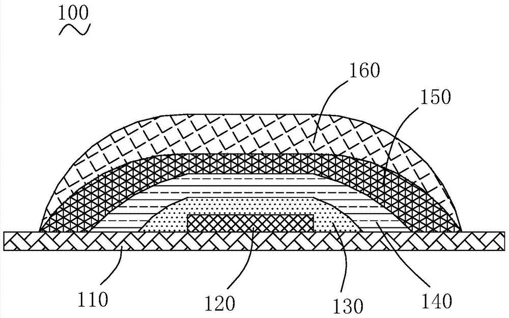
[0034] Please refer to figure 1 , the light-emitting device 100 according to Embodiment 1 of the present invention includes a substrate 110, an organic light-emitting element 120 disposed on the substrate 110, an inorganic material layer 130 covering the organic light-emitting element 120, an organic material layer 140 covering the inorganic material layer 130, and an organic light-emitting element covering the organic light-emitting element 120. The resin film layer 150 of the material layer 140 , and the inorganic sealing layer 160 covering the resin film layer 150 .
[0035] In this embodiment, the inorganic material layer 130 is deposited on the organic light-emitting element 120 first, wherein the inorganic material can be inorganic nitride or inorganic oxide, such as aluminum oxide, silicon oxide, silicon nitride, zirconium oxide, and titanium oxide. The organic material layer 140 is arranged on the inorganic material layer 130, which is adjacent to the resin film layer ...
Embodiment 2
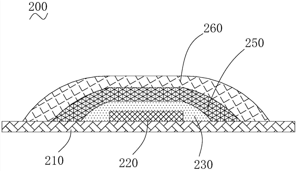
[0046] Please refer to image 3 , the light-emitting device 200 of Embodiment 2 of the present invention includes a substrate 210, an organic light-emitting element 220 disposed on the substrate 210, an inorganic material layer / organic material layer 230 covering the organic light-emitting element 220, an inorganic material layer / organic material layer 230 covering the The resin film layer 250, and the inorganic sealing layer 260 covering the resin film layer 250.
[0047] In this embodiment, the only difference from Embodiment 1 is: In the inorganic material layer / organic material layer 230, the inorganic material layer and the organic material layer are alternately arranged in multiple layers, all of which are more than two layers, multi-layer inorganic material layers The organic material layer can further improve the encapsulation effect. In addition, the manufacturing process of the light-emitting device 200 is the same as that of the light-emitting device 100 , the only...
Embodiment 3
[0050] Please refer to Figure 4 , the light-emitting device 300 of Embodiment 3 of the present invention includes a substrate 310, an organic light-emitting element 320 disposed on the substrate 310, an inorganic material layer / organic material layer 330 covering the organic light-emitting element 320, an inorganic material layer / organic material layer 330 covering the The resin film layer 350, and the inorganic sealing layer 360 covering the resin film layer 350.
[0051] The structure of the light emitting device 300 is similar to that of the light emitting device 200 , the difference is that in Embodiment 3, a transparent water absorbing layer 370 is provided between the resin film layer 350 and the inorganic material layer / organic material layer 330 . The transparent water-absorbing layer 370 is made of transparent water-absorbing materials such as acrylic resin or silicon monoxide, which can absorb a small amount of water vapor entering the resin film layer 350, thereby ...
PUM
 Abstract
Description
Claims
Application Information
 - R&D
- Intellectual Property
- Life Sciences
- Materials
- Tech Scout
- Unparalleled Data Quality
- Higher Quality Content
- 60% Fewer Hallucinations
Browse by: Latest US Patents, China's latest patents, Technical Efficacy Thesaurus, Application Domain, Technology Topic, Popular Technical Reports.
© 2025 PatSnap. All rights reserved.Legal|Privacy policy|Modern Slavery Act Transparency Statement|Sitemap|About US| Contact US: help@patsnap.com