Manufacturing method of high-alignment HDI (High Density Interconnection) product

A manufacturing method and technology of alignment degree, which can be used in multilayer circuit manufacturing, printed circuit manufacturing, and electrical connection formation of printed components. problems, to achieve the effect of improving the alignment between boards, improving the pass rate, and increasing the efficiency of the enterprise

Active Publication Date: 2015-04-22
东莞康源电子有限公司
View PDF5 Cites 13 Cited by
  • Summary
  • Abstract
  • Description
  • Claims
  • Application Information

AI Technical Summary

Problems solved by technology

[0003] However, with the development of HDI technology, there are more and more layers of product production, and HDI mostly relies on blind holes for conduction. With the increase of product layers, the number of blind hole layers is also increasing. The traditional blind The hole alignment method uses the target hole or th

Method used


Image

  • Manufacturing method of high-alignment HDI (High Density Interconnection) product
  • Manufacturing method of high-alignment HDI (High Density Interconnection) product
  • Manufacturing method of high-alignment HDI (High Density Interconnection) product

Examples


Embodiment Construction

[0023] In order to make the technical solution of the present invention more clearly expressed, the present invention will be further described below in conjunction with the accompanying drawings.

[0024] like Figure 1 to Figure 13 As shown, the present invention provides a kind of manufacturing method of high alignment HDI product, comprises the following steps:

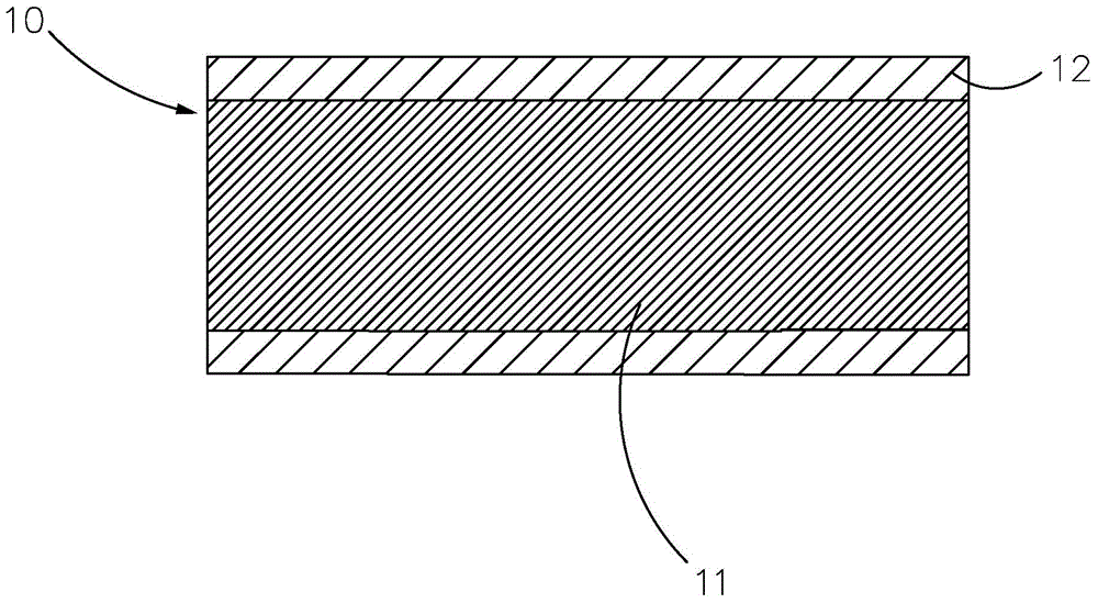
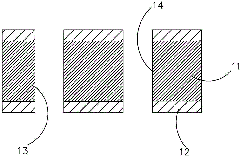
[0025] Step (1): making an inner core board 10, the inner core board 10 includes a flexible layer 11 and a copper layer 12 pressed up and down on the flexible layer 11;

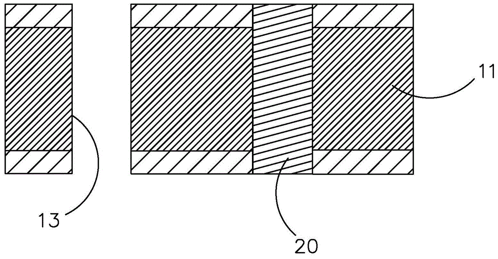
[0026] Step (2): Drilling a through hole 14 and a first alignment hole 13 on the inner core board 10 by means of mechanical drilling;

[0027] Step (3): filling the holes, using the resin 20 to plug the through holes 14, so that the resin 20 fills the through holes 14;

[0028] Step (4): Copper electroplating, copper plating on the upper and lower surfaces of the inner core board 10 to form a copper clad layer 30, the copper clad layer 30 cover...


PUM


Abstract

The invention discloses a manufacturing method of a high-alignment HDI (High Density Interconnection) product. The method comprises the following steps: forming an annular groove in an inner-layer pattern, wherein the annular groove is formed concentrically with a first registration hole, and is used for judging whether the practical position of the first registration hole corresponds to the practical position of the inner-layer pattern or not by judging whether the substantial position of the first registration hole is concentric with the substantial position of the annular groove or not; and repeatedly drilling overlapped boards, aligning the boards through the first registration hole and a second registration hole, and determining the position of a blind hole by taking the first registration hole and the second registration hole as registration points. Through adoption of the manufacturing method, the inter-board alignment of PCBs (Printed Circuit Boards) is effectively enhanced; the yield during board manufacturing is increased; and the enterprise benefit is increased.

Description

technical field [0001] The invention relates to the technical field of circuit boards, in particular to a method for manufacturing high-alignment HDI products. Background technique [0002] With the current trend of continuous and rapid miniaturization, portability and multi-functionalization of electronic products, and the development of high-density mounting technology, the industry has increasingly put forward higher requirements for the carrier and connector printed circuit board as the original component. , so that it can become an electronic component with high density, high precision, and high reliability that can greatly increase the assembly density. Therefore, the high density interconnection (high density interconnection, HDI) applied to the new PCB process technology is widely used in various electronic products, and the application range of the HDI board technology is becoming wider and wider. [0003] However, with the development of HDI technology, there are ...

Claims


Application Information

Patent Timeline
IPC IPC(8): H05K3/46H05K3/40
CPCH05K3/421H05K3/429H05K3/465H05K2201/0959H05K2201/096
Inventor 龚正杨建勇
Owner 东莞康源电子有限公司
Why Eureka
Try Eureka