
Mask plate and method for reducing splicing exposure mula phenomenon

A mask plate and mask plate technology, applied in the field of photolithography, can solve problems such as splicing exposure mura, exposure alignment error, and complex manufacturing process of TFT array substrates, so as to reduce the difference in display brightness, improve picture quality, and eliminate shadowing. pull effect

Inactive Publication Date: 2015-04-29
HEFEI BOE OPTOELECTRONICS TECH +1
View PDF12 Cites 26 Cited by
  • Summary
  • Abstract
  • Description
  • Claims
  • Application Information

AI Technical Summary

Problems solved by technology

[0003] In order to meet the needs of large-area display, the size of TFT liquid crystal display panels is getting larger and larger, which makes the manufacturing process of TFT array substrates more and more complicated.
In order to increase the size of the TFT array substrate, the size of the reticle also needs to be increased accordingly. However, due to the limitation of the exposure machine on the size of the reticle, and the large-size reticle has problems such as manufacturing difficulties, high cost, and inconvenient daily storage and use. , so that when manufacturing the TFT array substrate, it is necessary to divide the large-size array substrate into several regions, and make the corresponding mask part of each region, and use these masks to expose the regions in the manufacturing process, and finally assemble a large-sized TFT Array substrate
[0004] At present, in the process of manufacturing TFT array substrates by splicing exposure, due to the exposure alignment error of the exposure machine in the factory, it is inevitable that the pattern in the splicing area needs to be exposed twice or more repeatedly. However, , after the graphics are repeatedly exposed, their size will become smaller, and there are some differences compared with other graphics that have only been exposed once. This difference may lead to differences in the display screen after the LCD panel is completed, and then splicing exposure mla phenomenon

Method used


Image

  • Mask plate and method for reducing splicing exposure mula phenomenon
  • Mask plate and method for reducing splicing exposure mula phenomenon
  • Mask plate and method for reducing splicing exposure mula phenomenon

Examples


Embodiment Construction

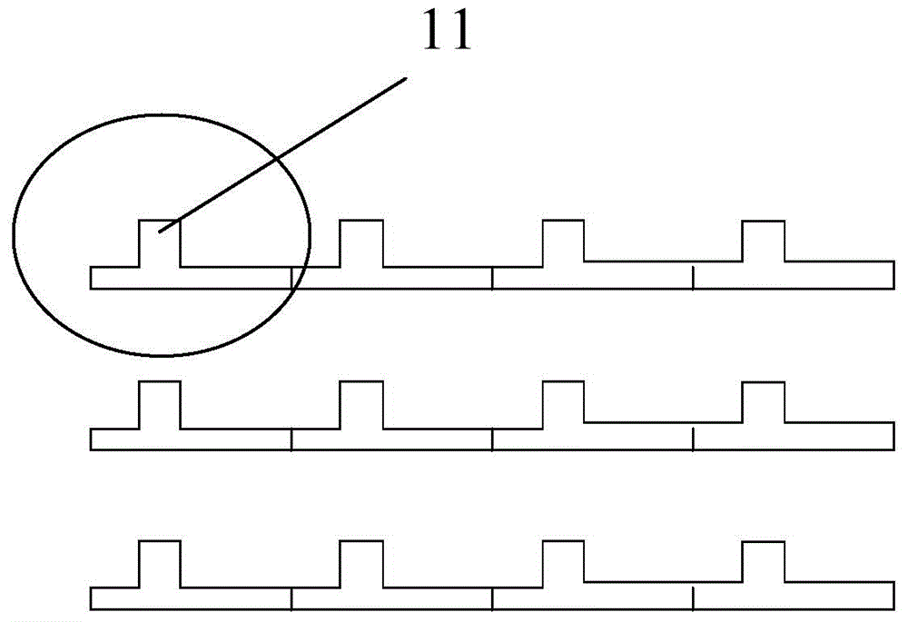
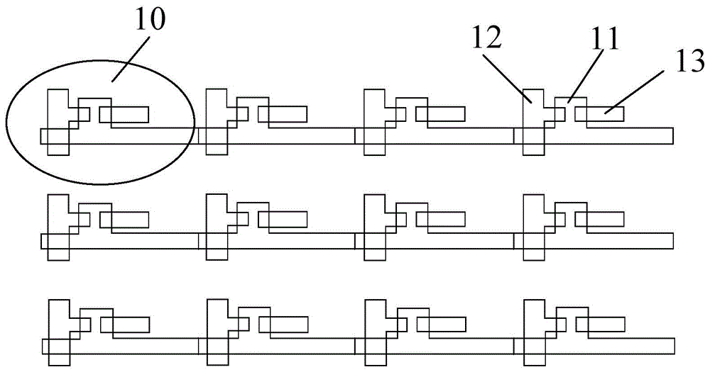
[0027] A mask plate provided by an embodiment of the present invention is applied to fabricate an array substrate by splicing exposure, and the array substrate includes a plurality of pattern areas and splicing areas between adjacent pattern areas; it is characterized in that, The mask plate includes: a plurality of complete transmission regions and partial transmission regions between adjacent complete transmission regions; wherein, the complete transmission regions correspond to pattern regions on the array substrate, and the partial transmission regions The area corresponds to the splicing area on the array substrate, and the width of the partial transmission area is greater than the width of the splicing area.

[0028] Here, the width of the partial transmission area is the sum of the width of the stitching area and twice the alignment accuracy between the mask plate and the array substrate.

[0029] Here, the exposure rate of the partially transmissive region is n / n, wher...


PUM

PropertyMeasurementUnit
Thicknessaaaaaaaaaa

Abstract

The invention discloses a mask plate which is used for manufacturing an array base plate in a splicing explosion mode, and the array base plate comprises a plurality of graph areas and splicing areas among adjacent graph areas. The mask plate comprises a plurality of complete transmission areas and partial transmission areas among adjacent complete transmission areas, wherein the complete transmission areas correspond to the graph areas on the array base plate; the partial transmission areas correspond to the splicing areas on the array base plate; the widths of the partial transmission areas are greater than those of the splicing areas. The invention further discloses a method for reducing the splicing exposure mula phenomenon. By adopting the technical scheme, the splicing exposure mula phenomenon can be effectively reduced or even eliminated, the display brightness difference of the splicing areas is reduced, and thus the image quality of a liquid crystal panel manufactured in a splicing explosion mode is improved.

Description

technical field [0001] The invention relates to the technical field of photolithography, in particular to a mask plate and a method for improving the Mural phenomenon of splicing exposure. Background technique [0002] The information society increasingly needs thin, light and portable display devices. At present, the more mature products are thin film transistor (TFT, Thin Film Transistor) liquid crystal displays. A TFT liquid crystal display is mainly composed of a TFT array substrate, an opposing color filter substrate, and a liquid crystal layer sandwiched between the two substrates. Wherein, the TFT array substrate mainly includes an array substrate, and a gate metal layer, a gate insulating layer, a semiconductor layer, a source-drain metal layer, an insulating film protection layer, and a transparent pixel layer stacked on the array substrate. The manufacturing process of the TFT array substrate is to transfer the pattern on the mask plate to the substrate through mu...

Claims


Application Information

Patent Timeline
IPC IPC(8): G03F7/20G03F9/00G03F1/48
Inventor 曾勉涂志中
Owner HEFEI BOE OPTOELECTRONICS TECH
Learn More