Wafer cooling tray
A tray and wafer technology, applied in electrical components, semiconductor/solid-state device manufacturing, circuits, etc., can solve the problems of reduced work efficiency, poor cooling effect, inconvenience in picking and placing wafers, etc., to improve cooling efficiency, facilitate transportation, clamping Easy to put and take effect
- Summary
- Abstract
- Description
- Claims
- Application Information
AI Technical Summary
Problems solved by technology
Method used
Image
Examples
Embodiment Construction
[0016] The following will clearly and completely describe the technical solutions in the embodiments of the present invention. Obviously, the described embodiments are only some of the embodiments of the present invention, rather than all the embodiments. Based on the embodiments of the present invention, all other embodiments obtained by persons of ordinary skill in the art without making creative efforts belong to the protection scope of the present invention.
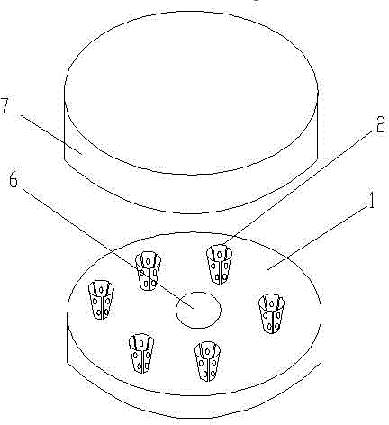
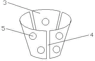
[0017] see figure 1 and figure 2 , the embodiment of the present invention includes:
[0018] A wafer cooling tray, comprising a tray body 1 and a plurality of wafer cooling stages 2 arranged on the tray body, the wafer cooling stages 2 are protrudingly arranged on the tray body 1, and the wafer cooling stages 2 are composed of three Arc-shaped pieces 3 are spliced together in a ring. The wafer cooling table 2 is an inverted circular frustum. The bottom of the arc-shaped pieces 3 is fixed on the tray body 1. The...
PUM
 Abstract
Description
Claims
Application Information
 - R&D
- Intellectual Property
- Life Sciences
- Materials
- Tech Scout
- Unparalleled Data Quality
- Higher Quality Content
- 60% Fewer Hallucinations
Browse by: Latest US Patents, China's latest patents, Technical Efficacy Thesaurus, Application Domain, Technology Topic, Popular Technical Reports.
© 2025 PatSnap. All rights reserved.Legal|Privacy policy|Modern Slavery Act Transparency Statement|Sitemap|About US| Contact US: help@patsnap.com


