Method for improving anti-interference capability of PCB, anti-interference PCB and terminal comprising anti-interference PCB

A technology for PCB boards and mobile terminals, applied in the reduction of crosstalk/noise/electromagnetic interference (, printed circuits, antennas, etc.) ability, the effect of improving anti-interference ability

Inactive Publication Date: 2015-04-29
ZTE CORP
View PDF3 Cites 3 Cited by
  • Summary
  • Abstract
  • Description
  • Claims
  • Application Information

AI Technical Summary

Problems solved by technology

This is also the reason why people often find that the power sensitivity of the cable test is normal in the project, but the coupling OTA test finds that the index is very poor.
During the development of terminal PCB boards, interference signals can be measured on the common ground of the main board of many terminal projects. Some of these interference signals are within the RF working frequency band, and the interference signals are radiated through the ground, which affects the coupling performance of the terminal and the radiation area. The distance to the antenna is very close. Once the radiated in-band signal is strong, it will have a great impact on the wireless performance of the terminal. The improvement of this problem through radio frequency debugging has little effect. This kind of fault is also a common occurrence faced by smart terminals. permanent failure, and even affect the success or failure of the project when the failure is serious
The interference of the PCB working antenna has brought a lot of troubles to the terminal project, and it is also very difficult to solve

Method used


Image

  • Method for improving anti-interference capability of PCB, anti-interference PCB and terminal comprising anti-interference PCB
  • Method for improving anti-interference capability of PCB, anti-interference PCB and terminal comprising anti-interference PCB
  • Method for improving anti-interference capability of PCB, anti-interference PCB and terminal comprising anti-interference PCB

Examples


Embodiment Construction

[0022] Hereinafter, the present invention will be further described in detail through specific embodiments in conjunction with the drawings.

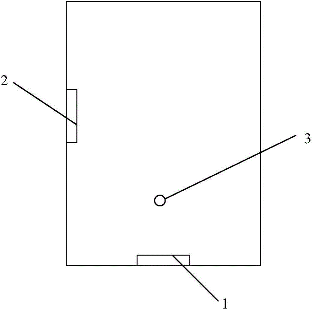
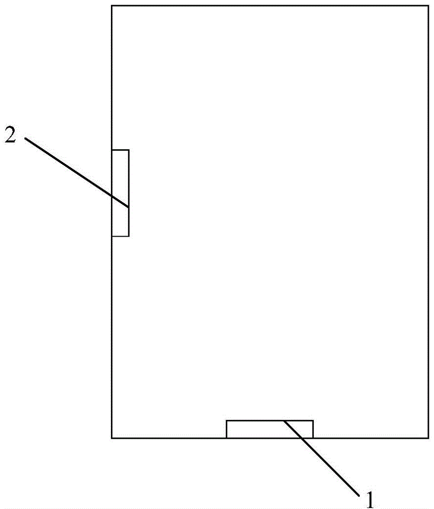
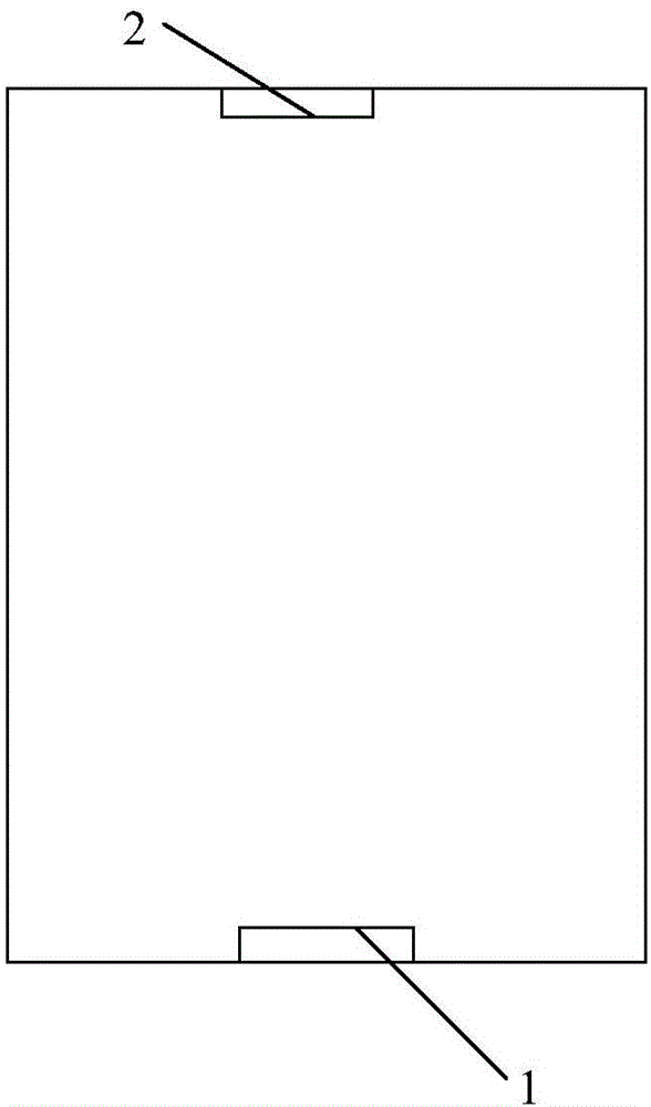
[0023] Such as figure 1 As shown, the present invention provides an anti-interference PCB board, which includes a working antenna, and is further provided with an anti-interference antenna. The impedance between the signal input end of the working antenna and the common ground of the PCB board is greater than the signal input of the anti-interference antenna The impedance between the terminal and the common ground of the PCB.

[0024] This embodiment proposes a radiation antenna that uses the mainboard common ground 2 as interference signals. When the mainboard common ground 2 is in operation due to various components on the mainboard, different interference signals will be generated, and the interference signals of different frequencies will all flow to the common ground. 2. The public ground 2 will radiate a lot of interference. When the w...


PUM


Abstract

Disclosed are a PCB board, a terminal and a method for improving an anti-interference capability of the PCB board. The method comprises: by setting an anti-interference antenna, enabling the impedance between a signal input terminal of an operation antenna of a PCB board and a common ground terminal of the PCB to be greater than the impedance between a signal input end of the anti-interference antenna and the common ground terminal.

Description

Technical field [0001] The invention relates to the field of PCB design, in particular to a method for improving the anti-interference of a PCB board and an anti-interference PCB board and its terminal. Background technique [0002] At present, PCB boards are more and more widely used. As PCBs have more and more functional application chips, their various baseband radio frequency chips are integrated on the same PCB motherboard, which causes the problem of electromagnetic mutual interference of PCB motherboards to be very prominent. On the common ground of the PCB board, we can often measure the interference signals of different frequency spectrums. These interference signals are radiated from the main board ground as the antenna. Some frequencies fall within the frequency band of the working antenna, which brings a lot to the working antenna signal. Interference. This is also the reason why people often find that the power sensitivity of the cable test is normal in the project,...

Claims


Application Information

Patent Timeline
Patent Type & Authority Applications(China)
IPC IPC(8): H01Q1/38H01Q1/50H01Q1/48H01Q23/00
CPCH01Q1/521H01Q1/50H05K1/0216H05K1/025H05K2201/10098
Inventor 罗玲程攀刚罗迤宝
Owner ZTE CORP
Why Eureka
Try Eureka