Semiconductor device and manufacturing method thereof

A manufacturing method and semiconductor technology, applied in semiconductor/solid-state device manufacturing, semiconductor devices, semiconductor/solid-state device components, etc., can solve problems such as short circuit of bonding materials, and achieve the effect of improving quality and reliability

Active Publication Date: 2018-07-03
MITSUBISHI ELECTRIC CORP
View PDF5 Cites 0 Cited by
  • Summary
  • Abstract
  • Description
  • Claims
  • Application Information

AI Technical Summary

Problems solved by technology

Therefore, in the manufacturing process subsequent to the process of bonding semiconductor elements, there is a problem that the overflowing bonding material falls off due to vibration or the like and causes problems such as short circuits.

Method used


Image

  • Semiconductor device and manufacturing method thereof
  • Semiconductor device and manufacturing method thereof
  • Semiconductor device and manufacturing method thereof

Examples


Embodiment approach 1

[0021]

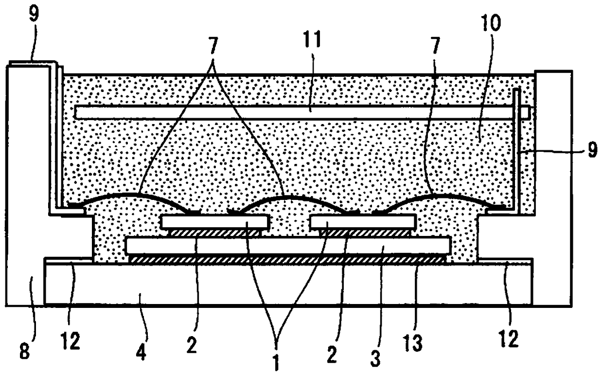
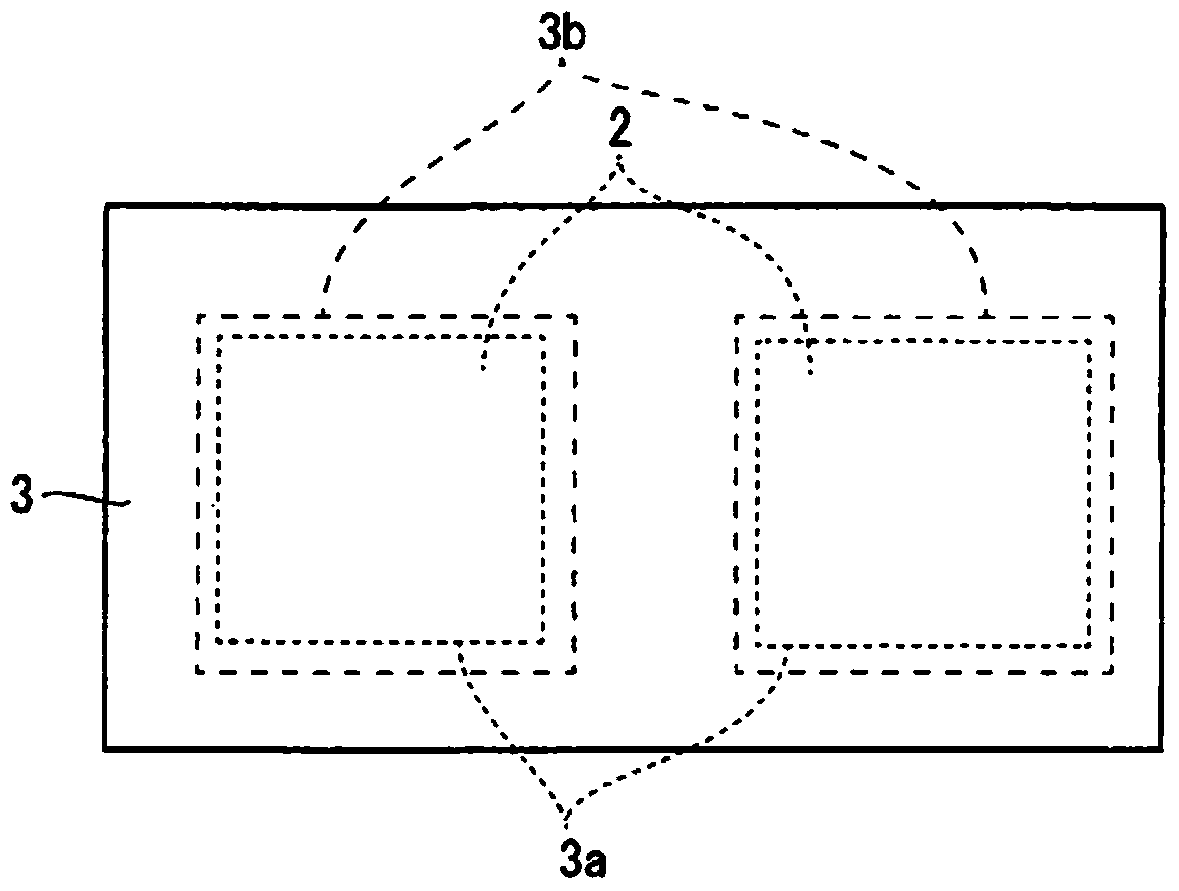
[0022] figure 1 A cross-sectional view showing a semiconductor module including the semiconductor device of the present embodiment is applied to an electronic device used in a high-temperature environment. The semiconductor device of the present embodiment includes: an insulating substrate 3 as an insulating substrate; a semiconductor element 1 to be bonded to the insulating substrate 3 ; and a sinterable bonding material 2 to bond the insulating substrate 3 and the semiconductor element 1 .

[0023] Insulating substrate 3 is bonded to heat sink 4 via solder 13 or a sinterable bonding material. The insulating substrate 3 has a circuit pattern on its surface. The circuit pattern on the surface of the insulating substrate 3 and the back electrode of the semiconductor element 1 are bonded by a sinterable bonding material 2 .

[0024] The heat dissipation plate 4 is fixed to the case 8 which becomes the outer contour of the semiconductor module with, for example, an a...

Embodiment approach 2

[0068]

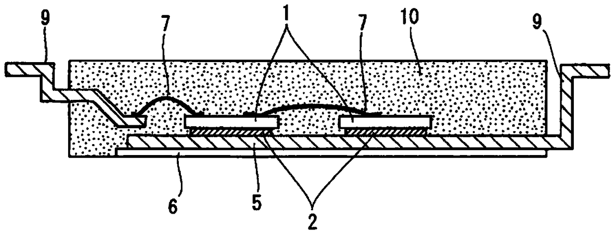
[0069] image 3 A cross-sectional view showing a semiconductor module including the semiconductor device of the present embodiment is applied to an electronic device used in a high-temperature environment. The semiconductor device of the present embodiment includes a conductive substrate 5 , a semiconductor element 1 bonded to the conductive substrate 5 , and a sinterable bonding material 2 bonded to the conductive substrate 5 and the semiconductor element 1 . In addition, the conductive substrate 5 is a metal plate.

[0070] The back surface of the conductive substrate 5 (ie, the surface opposite to the surface bonded to the semiconductor element 1 ) is fixedly bonded to the insulating metal layer 6 having an insulating foil on the bottom surface.

[0071] Such as image 3 As shown, an electrode 9 is provided at one end of the conductive substrate 5 . In addition, an electrode 9 on the other end side of the conductive substrate 5 is connected to an electrode on ...


PUM

PropertyMeasurementUnit
diameteraaaaaaaaaa
diameteraaaaaaaaaa
thicknessaaaaaaaaaa

Abstract

An object of the present invention is to provide a semiconductor device and a method for manufacturing the semiconductor device, which improve the high-temperature durability, quality, and reliability of a junction between a semiconductor element and a substrate by using a sinterable junction material. The semiconductor device manufacturing method of the present invention is characterized in that it includes the following steps: (a) preparing an insulating or conductive substrate; (b) disposing a sinterable bonding material in the bonding region (3a) of the main surface of the substrate (that is, an insulating substrate) (c) sintering the bonding material while making the surface for bonding of the semiconductor element, that is, the bonding surface, contact with the bonding material under pressure, thereby bonding the substrate (i.e., an insulating substrate) and the semiconductor element via the bonding material, the process ( The bonding region in b) is located inside the bonding surface of the semiconductor element (i.e., region (3b)) in plan view, and after step (c), the bonding material does not go outside the bonding surface of the semiconductor element in plan view. overflow.

Description

technical field [0001] The present invention relates to a semiconductor device and a manufacturing method thereof, in particular to a bonding method of semiconductor elements. Background technique [0002] In recent years, as environmental regulations have increased, there has been an increasing demand for electronic devices that take environmental issues into account (that is, electronic devices that achieve high quality, high efficiency, and energy saving). In particular, electronic equipment corresponding to high power is required for industrial equipment, drive control equipment for home appliances equipped with electric motors, on-board control equipment for electric vehicles and hybrid vehicles, railway vehicle control equipment, solar power generation control equipment, and the like. In addition, there is a demand for high efficiency and low loss in the operation of electronic equipment in a high-load environment (high-temperature environment). The so-called high-tem...

Claims


Application Information

Patent Timeline
Patent Type & Authority Patents(China)
IPC IPC(8): H01L21/603H01L23/488
CPCH01L24/29H01L24/83H01L24/32H01L24/45H01L24/48H01L24/73H01L24/85H01L2224/04042H01L2224/29014H01L2224/29007H01L2224/29339H01L2224/29344H01L2224/29364H01L2224/29347H01L2224/45015H01L2224/45124H01L2224/32055H01L2224/32014H01L2224/32225H01L2224/32245H01L2224/48137H01L2224/48472H01L2224/73265H01L2224/83203H01L2224/8384H01L2224/92247H01L2924/13055H01L2924/13091H01L2924/351H01L2924/181H01L2924/15787H01L2924/00H01L2924/00012H01L2924/2076H01L2924/00014H01L2224/48247
Inventor 日野泰成
Owner MITSUBISHI ELECTRIC CORP
Why Eureka
Try Eureka