Unsealing method of chip package
A chip packaging and packaging technology, applied in semiconductor/solid-state device manufacturing, electrical components, circuits, etc., can solve problems such as chip and lead damage, and achieve the effect of improving and avoiding damage.
- Summary
- Abstract
- Description
- Claims
- Application Information
AI Technical Summary
Problems solved by technology
Method used
Image

Examples
Embodiment 1
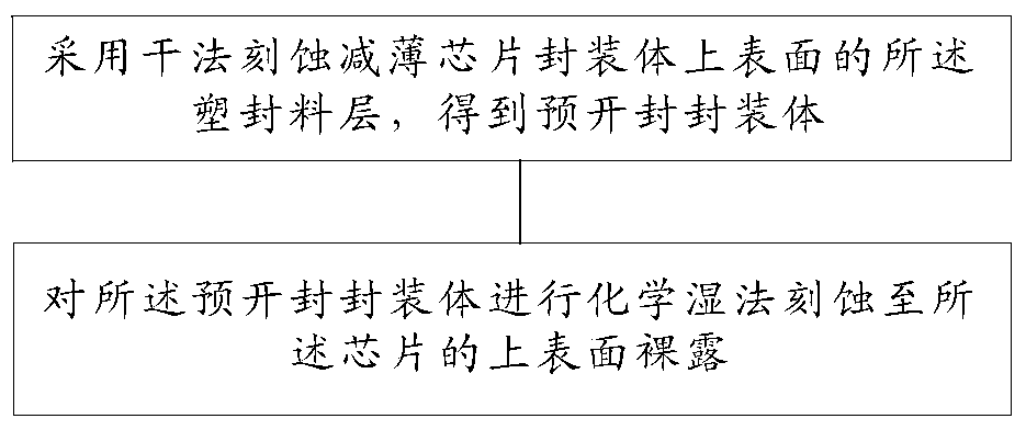
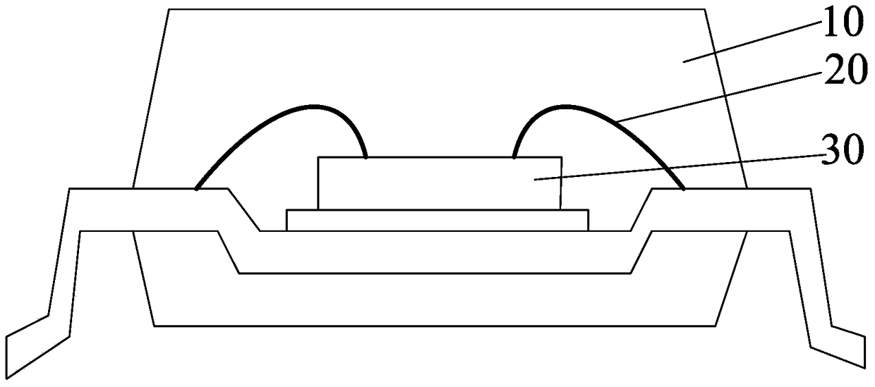
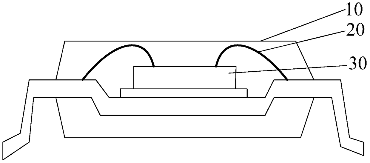
[0044] A plasma etching machine with the model Plasma lab80plus was used as the dry etching device. The excitation power of the plasma etching machine was set to 1000W, the bias voltage was 500V, and the etching gas was Ar and 5:2 in volume ratio. O 2 , the pressure of the etching gas is 100mT, the flow rate is 1000sccm, the etching time is 20min, and the etching rate is about 25μm / min. The thickness of the etched plastic sealing material layer is calculated by the etching rate and etching time. The top surface of the etched plastic material layer is 20 μm away from the highest point of the lead.
[0045] The chemical wet etching is carried out by using the unsealing device disclosed in the patent application with the application number of 200910056017.8, wherein the etching solution adopts a mixed acid solution composed of fuming nitric acid and 98% sulfuric acid in a volume ratio of 1:1, and the etching temperature is After 500s at 35° C., the top surface of the chip was ex...
Embodiment 2
[0047] A plasma etching machine with the model Plasma lab80plus was used as the dry etching device. The excitation power of the plasma etching machine was set to 1500W, the bias voltage was 100V, and the etching gas was Ar and 6:3 in volume ratio. O2, the pressure of the etching gas is 200mT, the flow rate is 800sccm, the etching time is 25min, and the etching rate is about 22μm / min. The thickness of the etched plastic sealant layer is calculated by the etching rate and etching time. The top surface of the etched plastic material layer is 12 μm away from the highest point of the lead.
[0048] Chemical wet etching is carried out by using the unsealing device disclosed in the patent application with the application number of 200910056017.8, wherein the etching solution adopts a mixed acid solution composed of fuming nitric acid and 98% sulfuric acid with a volume ratio of 1:3, and the etching temperature is The top surface of the chip was exposed after 500 s at 40° C., and was ...
Embodiment 3
[0050] A plasma etching machine with model Plasma lab80plus was used as the dry etching device. The excitation power of the plasma etching machine was set to 600W, the bias voltage was 800V, and the etching gas was Ar and 4:1 in volume ratio. O2, the pressure of the etching gas is 50mT, the flow rate is 1500sccm, the etching time is 15min, and the etching rate is about 30μm / min. The thickness of the etched plastic sealing material layer is calculated by the etching rate and etching time. The top surface of the etched plastic material layer is 30 μm away from the highest point of the lead.
[0051] Chemical wet etching is carried out by using the unsealing device disclosed in the patent application with the application number of 200910056017.8, wherein the etching solution adopts a mixed acid solution composed of fuming nitric acid and 98% sulfuric acid with a volume ratio of 1:2, and the etching temperature is After 600 s at 30° C., the top surface of the chip was exposed and ...
PUM
 Abstract
Description
Claims
Application Information
 - R&D Engineer
- R&D Manager
- IP Professional
- Industry Leading Data Capabilities
- Powerful AI technology
- Patent DNA Extraction
Browse by: Latest US Patents, China's latest patents, Technical Efficacy Thesaurus, Application Domain, Technology Topic.
© 2024 PatSnap. All rights reserved.Legal|Privacy policy|Modern Slavery Act Transparency Statement|Sitemap