Interface structure and configuration method of FPGA (field programmable gate array) chip

An interface structure and chip technology, applied in instruments, computer control, simulators, etc., can solve the problems of limited number of input and output units, large area of ​​input and output units, unfavorable small size of chips, etc. Effects of timing requirements

Active Publication Date: 2015-06-03
CAPITAL MICROELECTRONICS
View PDF6 Cites 3 Cited by
  • Summary
  • Abstract
  • Description
  • Claims
  • Application Information

AI Technical Summary

Problems solved by technology

[0003] In traditional FPGA chips, the registers in the fast input and output FastIO interface unit are all configured inside the input and output unit, so the area of ​​the input and output unit will be relatively large. As a result, in the FPGA chip, due to the limitation of the area, the input and output The number of units is limited
At the same time, the large input and output unit area is not conducive to the small size of the chip

Method used


Image

  • Interface structure and configuration method of FPGA (field programmable gate array) chip
  • Interface structure and configuration method of FPGA (field programmable gate array) chip
  • Interface structure and configuration method of FPGA (field programmable gate array) chip

Examples


Embodiment Construction

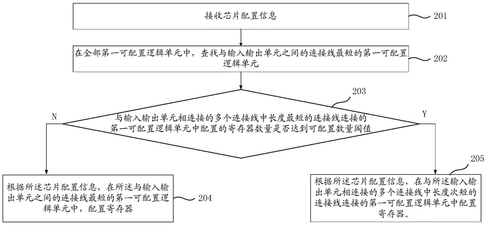
[0024] The technical solutions of the present invention will be described in further detail below with reference to the accompanying drawings and embodiments.

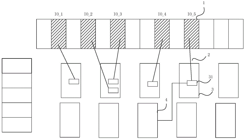
[0025] figure 1 It is a schematic diagram of the interface structure of the FPGA chip provided by the embodiment of the present invention. As shown in the figure, the interface structure of the FPGA chip includes: an input-output (IO) unit 1 , a connection line 2 and a first configurable logic unit 3 .

[0026] The input and output unit 1 is connected to an external chip or circuit, and is used to receive chip configuration information sent from the outside; wherein, the chip configuration information is information used to configure each logic unit inside the FPGA chip.

[0027] The connection line 2 is used to connect the input and output unit 1 and each unit inside the FPGA chip, including the first configurable logic unit 3 or the second configurable logic unit 4; in addition, between each unit inside the FPGA chi...


PUM


Abstract

The invention relates to an interface structure and a configuration method of an FPGA (field programmable gate array) chip. The structure comprises an input and output unit, connecting wires and a first configurable logic unit, wherein the input and output unit is used for receiving chip configuration information sent by the outside, the first configurable logic unit is connected with the input and output unit through the connecting wire, and in addition, a register is configured in the first configurable logic unit connected with the shortest connecting wire in the plurality of connecting wires connected with the input and output unit according to the chip configuration information received by the input and output unit.

Description

technical field [0001] The invention relates to the technical field of field programmable logic gate array (Field Programmable Gate Array, FPGA) chip configuration structure technology, in particular to the interface structure and configuration method of the FPGA chip. Background technique [0002] FPGA is a logic device with abundant hardware resources, powerful parallel processing capability and flexible reconfigurable capability. These features make FPGA more and more widely used in data processing, communication, network and many other fields. [0003] In traditional FPGA chips, the registers in the fast input and output FastIO interface unit are all configured inside the input and output unit, so the area of ​​the input and output unit will be relatively large. As a result, in the FPGA chip, due to the limitation of the area, the input and output The number of units is limited. At the same time, the large input and output unit area is not conducive to the miniaturizat...

Claims


Application Information

Patent Timeline
Patent Type & Authority Applications(China)
IPC IPC(8): G05B19/042
CPCG05B19/0423
Inventor 虞健蒋中华吴鑫刘明
Owner CAPITAL MICROELECTRONICS
Why Eureka
Try Eureka