Supercharge Your Innovation With Domain-Expert AI Agents!

Optoelectronic device and method for its manufacture

A technology of optoelectronic devices and quantum membranes, which is applied to electrical components, semiconductor devices, circuits, etc., and can solve the problems of quantum membranes with reduced efficiency

Active Publication Date: 2017-09-08
OSRAM OPTO SEMICON GMBH & CO OHG
View PDF10 Cites 0 Cited by
  • Summary
  • Abstract
  • Description
  • Claims
  • Application Information

AI Technical Summary

Problems solved by technology

[0006] Here, the efficiency drop rises with the number of quantum membranes

Method used


Image

  • Optoelectronic device and method for its manufacture
  • Optoelectronic device and method for its manufacture
  • Optoelectronic device and method for its manufacture

Examples


Embodiment Construction

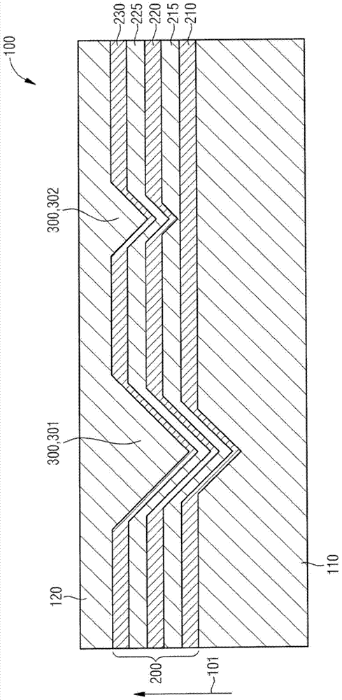
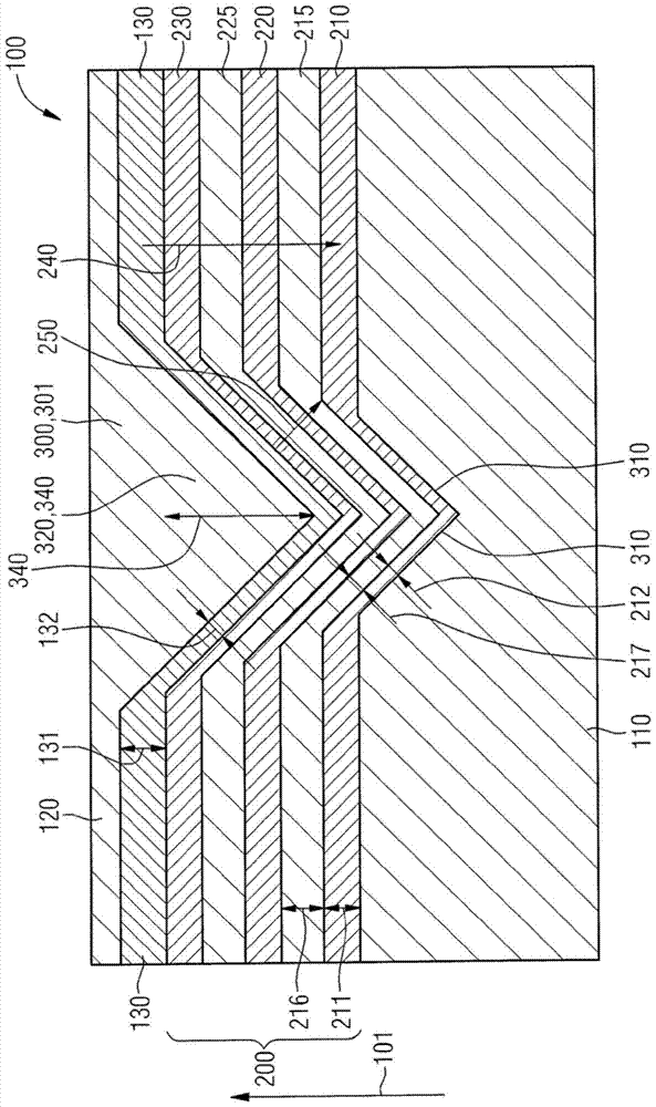
[0047] figure 1 A schematic diagram of a section through a part of the layer structure 100 is shown. Layer structure 100 is an epitaxially grown semiconductor layer structure. In particular, the layer structure 100 can consist of a III-nitride material system. The layer structure 100 can be used in optoelectronic components, in particular in light-emitting diodes.

[0048] Along the epitaxial growth direction 101 , an n-doped crystal 110 , an optically active layer 200 and a p-doped crystal 120 are located successively in the layer structure 100 . The layer structure 100 can be set in figure 1 on a substrate not shown. of the substrate and layer structure 100 in the figure 1 Other layers can also be arranged between the parts shown in . Further layers can also be arranged between the layers 110 , 200 , 120 of the layer structure 100 .

[0049] The optically active layer 200 has a plurality of quantum films which follow one another in the growth direction 101 and are eac...


PUM


Abstract

An optoelectronic component comprising a layer structure with an optically active layer. In this case, the optically active layer has a higher V-shaped defect density in the first lateral region than in the second lateral region.

Description

technical field [0001] The invention relates to an optoelectronic component and a method for producing an optoelectronic component. [0002] Cross-References to Related Applications [0003] This application claims priority from German patent application 102012217640.3, the disclosure of which is incorporated herein by reference. Background technique [0004] In light-emitting diodes based on semiconductors composed of III-nitride material systems, such as InGaN-GaN and having an active region composed of multiple quantum films (Multi-Quantum-Well; MQW, multiple quantum wells), in the current The prior art shows the problem that not all quantum membranes work together optimally and uniformly. This causes a loss of efficiency for such light-emitting diodes. [0005] The charge carrier distribution over the plurality of quantum films is obtained by injecting charge carriers into the quantum films along the growth direction of the semiconductor layer structure. It is desira...

Claims


Application Information

Patent Timeline
Patent Type & Authority Patents(China)
IPC IPC(8): H01L33/06
CPCH01L33/06H01L33/14H01L33/007H01L33/025H01L33/24H01L33/32H01L33/58H01L33/0025H01L33/0075
Inventor 克里斯蒂安·莱雷尔托比亚斯·迈耶马蒂亚斯·彼得于尔根·奥弗约阿希姆·赫特功安德烈亚斯·莱夫勒亚历山大·沃尔特达里奥·斯基亚翁
Owner OSRAM OPTO SEMICON GMBH & CO OHG
Features
  • R&D
  • Intellectual Property
  • Life Sciences
  • Materials
  • Tech Scout
  • Unparalleled Data Quality
  • Higher Quality Content
  • 60% Fewer Hallucinations
Learn More