Array substrate and manufacturing method thereof and touch detecting method of touch display device

An array substrate, self-capacitance touch technology, applied in the input/output process of data processing, instruments, calculations, etc., can solve the problems of touch sensitivity drop, touch resolution drop, etc., to achieve a good touch experience, reduce The effect of small touch response time and high detection resolution

Active Publication Date: 2015-06-10
SHANGHAI AVIC OPTOELECTRONICS +1
View PDF4 Cites 5 Cited by
  • Summary
  • Abstract
  • Description
  • Claims
  • Application Information

AI Technical Summary

Problems solved by technology

Normally, if you want to increase the touch resolution, the touch sensitivity will de

Method used


Image

  • Array substrate and manufacturing method thereof and touch detecting method of touch display device
  • Array substrate and manufacturing method thereof and touch detecting method of touch display device
  • Array substrate and manufacturing method thereof and touch detecting method of touch display device

Examples


Embodiment Construction

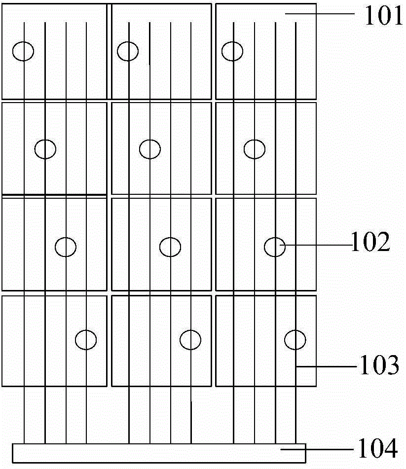
[0020] The inventor analyzed the in-cell touch screen based on the self-capacitance principle in the prior art, and found that in the in-cell touch screen based on the self-capacitance principle, the size of each self-capacitance touch electrode on the array substrate is consistent. figure 1 is a schematic diagram of an existing array substrate, such as figure 1 As shown, a plurality of electrodes 101 with the same area are provided in the conventional array substrate, and the electrodes 101 are electrically connected to the chip 104 through wires 103 in one-to-one correspondence. Wherein, each trace 103 is electrically connected to a corresponding electrode 101 through a via hole 102 on an insulating layer (not shown).

[0021] In order to ensure higher touch sensitivity, the size of existing self-capacitance touch electrodes is usually relatively large. For example figure 1 In the electrode 101 in, the length of each side is about 4 mm. If a finger is used for touch, sinc...


PUM


Abstract

Disclosed are an array substrate and a manufacturing method thereof and a touch detecting method of a touch display device. The array substrate comprises a self-capacitance touch electrode layer also used as a public electrode layer. The self-capacitance touch electrode layer comprises first electrodes and second electrodes, the area of each first electrode is smaller than that of each second electrode, and multiple first electrodes make up an electrode cluster in the outline shape same as that of the second electrodes. Both touch sensitivity and resolution of the array substrate can be up to high level.

Description

technical field [0001] The present invention relates to the display field, in particular to an array substrate and a forming method thereof, and a touch detection method of a touch display device. Background technique [0002] Liquid crystal display (liquid crystal display, LCD) or organic light-emitting diode (Organic Light-Emitting Diode, OLED) display has the advantages of low radiation, small size and low power consumption, etc., and is widely used in notebook computers, personal digital assistants (Personal Digital Assistants). Assistant, PDA), flat-screen TV, or information products such as mobile phones. [0003] Display technology integrated with touch technology has gradually spread into people's lives. At present, touch screens can be divided into three types according to their composition structures: external touch screens, surface-covering touch screens, and built-in touch screens. Among them, the embedded touch screen embeds the touch electrodes of the touch s...

Claims


Application Information

Patent Timeline
IPC IPC(8): G06F3/044
CPCG06F3/044G02F1/13338G06F3/0412G06F3/04164G06F3/04166G06F3/0443G06F3/0448G06F2203/04103
Inventor 金慧俊黄忠守叶松
Owner SHANGHAI AVIC OPTOELECTRONICS
Why Eureka
Try Eureka