Pixel definition layer of light-emitting display and its manufacturing method
A pixel definition layer and light-emitting display technology, which is applied in semiconductor/solid-state device manufacturing, photovoltaic power generation, electric solid-state devices, etc., can solve problems such as cathode-anode short circuit, light-emitting area reduction, and cathode discontinuous light-emitting area reduction, so as to facilitate the manufacturing process , The effect of improving light and color efficiency
- Summary
- Abstract
- Description
- Claims
- Application Information
AI Technical Summary
Problems solved by technology
Method used
Image
Examples
Embodiment approach 1
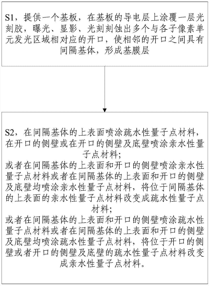
[0044] Manufacturing method embodiment 1, this embodiment takes the manufacturing of a pixel defining layer composed of three sub-pixels as an example, and the specific steps are as follows:
[0045] As attached Figure 4 As shown, a substrate 1 is provided, and a layer of positive photoresist 11 is coated on the conductive layer of the substrate 1. In this embodiment, the substrate 1 uses but is not limited to conductive glass. The conductive glass is formed by forming a layer of transparent conductive oxide on the upper surface of the transparent glass by means of sputtering or ion electrophoresis. The oxide is oxide. Indium tin, aluminum zinc oxide, indium zinc oxide.
[0046] Such as Figure 5 As shown, after exposing and developing the positive photoresist 11, a mask is used to lithographically etch a plurality of openings 3 corresponding to the light-emitting regions of each sub-pixel unit on the positive photoresist, so that adjacent There is a spacer matrix 4 between the o...
Embodiment approach 2
[0049] The second embodiment of the manufacturing method, this embodiment takes the manufacturing of a pixel defining layer composed of three sub-pixels as an example, and the specific steps are as follows:
[0050] Such as Picture 8 As shown, a substrate 1 is provided, and a layer of negative photoresist 12 is coated on the conductive layer of the substrate 1.
[0051] Such as Picture 9 As shown, after exposing and developing the negative photoresist 12, a mask is used to lithographically etch a plurality of openings 3 corresponding to the light-emitting regions of each sub-pixel unit on the negative photoresist 12 to make the A spacer base 4 is provided between adjacent openings 3 to form a base film layer 2. The longitudinal section of the spacer base 4 is an inverted trapezoid.
[0052] Such as Picture 10 As shown, the upper surface of the spacer substrate 4 and the side walls and bottom walls of the opening 3 are sprayed with a hydrophobic quantum dot material 5, and the si...
Embodiment approach 3
[0055] The third embodiment is different from the embodiment in that: the upper surface of the spacer substrate and the side wall of the opening are sprayed with hydrophilic quantum dot material, or the upper surface of the spacer substrate and the side wall and bottom wall of the opening are sprayed with hydrophilicity. The quantum dot material uses the replacement of functional groups to change the hydrophilic quantum dot material on the upper surface of the spacer into a hydrophobic quantum dot material.
[0056] It should be noted that the spraying of the present invention adopts nozzle spraying or arc spraying.
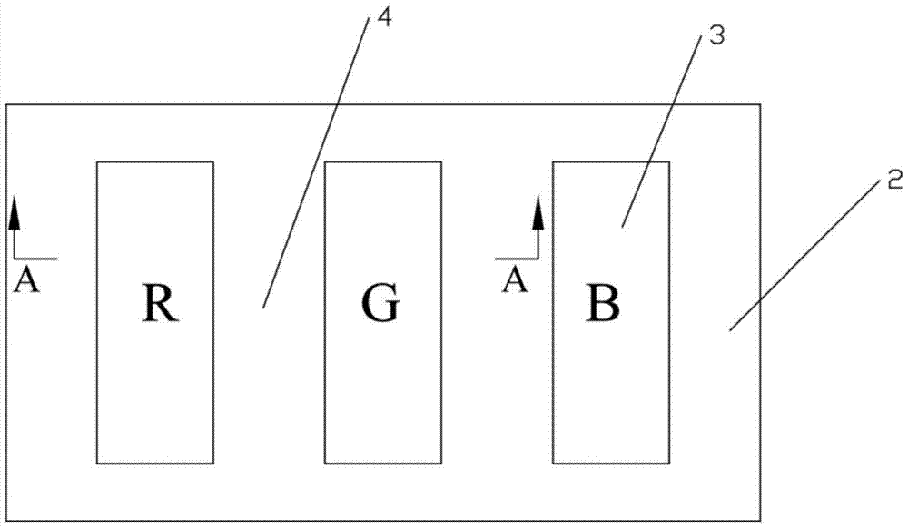
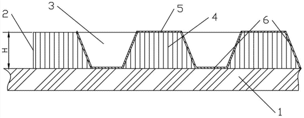
[0057] The pixel defining layer manufactured according to the above method for manufacturing the pixel defining layer includes a base film layer, and the sidewalls of the opening of the base film layer or the sidewalls and bottom walls of the opening are coated with a hydrophilic quantum dot material, and The upper surface of the spacer substrate is coated with hydrop...
PUM
 Abstract
Description
Claims
Application Information


