Pixel defining layer of light emitting display and manufacturing method thereof

A pixel-defining layer, light-emitting display technology, applied in semiconductor/solid-state device manufacturing, photovoltaic power generation, electric solid-state devices, etc., can solve the problems of short circuit of cathode and anode, reduction of light-emitting area, reduction of discontinuous light-emitting area of ​​cathode, etc., which is beneficial to the process. , the effect of improving light and color efficiency

Active Publication Date: 2015-06-24
BOE TECH GRP CO LTD
View PDF3 Cites 63 Cited by
  • Summary
  • Abstract
  • Description
  • Claims
  • Application Information

AI Technical Summary

Problems solved by technology

[0004] In the current positive trapezoidal pixel definition layer, the spreading effect of the organic layer after the hydrophobic treatment of the pixel definition layer is poor, and there will be an unspread area at the edge of the conductive glass and the pixel definition layer. After the cathode is evaporated, it is easy to cause a short circuit between the cathode and the anode, resulting in leakage.
The inverted trapezoidal pixel boundary layer will make the spread of the in

Method used


Image

  • Pixel defining layer of light emitting display and manufacturing method thereof
  • Pixel defining layer of light emitting display and manufacturing method thereof
  • Pixel defining layer of light emitting display and manufacturing method thereof

Examples


Embodiment approach 1

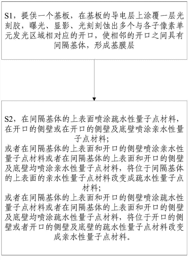
[0044] Embodiment 1 of the manufacturing method. This embodiment takes manufacturing a pixel definition layer of a pixel composed of three sub-pixels as an example. The specific steps are as follows:

[0045] like attached Figure 4 As shown, a substrate 1 is provided, and a layer of positive photoresist 11 is coated on the conductive layer of the substrate 1 . In this embodiment, the substrate 1 uses, but is not limited to, conductive glass, and the conductive glass is made of transparent glass above table The surface is formed by sputtering or ionic transfer to form a layer of transparent and conductive oxides. The oxides are indium tin oxide, aluminum zinc oxide, and indium zinc oxide.

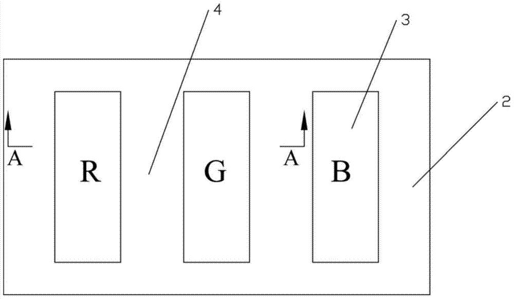
[0046] like Figure 5 As shown, after exposing and developing the positive photoresist 11, a plurality of openings 3 corresponding to the light-emitting regions of each sub-pixel unit are photoetched on the positive photoresist using a mask, so that adjacent A spacer matrix 4 is prov...

Embodiment approach 2

[0049] Embodiment 2 of the manufacturing method. This embodiment takes manufacturing a pixel definition layer of a pixel composed of three sub-pixels as an example. The specific steps are as follows:

[0050] like Figure 8 As shown, a substrate 1 is provided, and a layer of negative photoresist 12 is coated on the conductive layer of the substrate 1 .

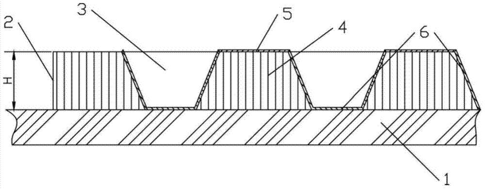
[0051] like Figure 9 As shown, after exposing and developing the negative photoresist 12, a mask plate is used to photoetch a plurality of openings 3 corresponding to the light-emitting regions of each sub-pixel unit on the negative photoresist 12, so that the corresponding A spacer matrix 4 is provided between adjacent openings 3 to form a base film layer 2 . The longitudinal section of the spacer base 4 is an inverted trapezoid.

[0052] like figure 1 0, in spacer matrix 4 of the above table The surface and the side walls and bottom walls of the opening 3 are sprayed with hydrophobic quantum dot materials 5, and...

Embodiment approach 3

[0055] The difference between the third embodiment and the embodiment is that: in the spacer matrix above table The surface and the sidewall of the opening are sprayed with hydrophilic quantum dot material or in the spacer matrix above table The surface and the side wall and bottom wall of the opening are sprayed with hydrophilic quantum dot materials, and the quantum dots located in the spacer matrix are replaced by functional groups. above table The hydrophilic quantum dot material on the surface is changed into a hydrophobic quantum dot material.

[0056] It should be noted that the spraying of the present invention adopts the mode of nozzle spraying or electric arc spraying.

[0057] According to the pixel defining layer made by the above method for making the pixel defining layer, the pixel defining layer includes a base film layer, and the side walls of the opening of the base film layer or the side walls and bottom walls of the opening are coated with hydrophilic quant...


PUM

PropertyMeasurementUnit
Heightaaaaaaaaaa
Heightaaaaaaaaaa

Abstract

The invention relates to the technical field of display, and discloses a pixel defining layer of a light emitting display. The pixel defining layer is arranged on a conducting layer of a substrate. The pixel defining layer is characterized in that a base film layer is included; the base film layer is provided with multiple openings corresponding to sub-pixel unit light emitting areas, and an interval matrix is formed between every two adjacent openings; the upper surface of each interval matrix is provided with hydrophobe quantum dot materials, and the side wall of each opening is provide with hydrophilic quantum materials. The invention further provides a manufacturing method of the pixel defining layer of the light emitting display. According to the pixel defining layer of the light emitting display and the manufacturing method thereof, it is guaranteed that ink in pixels cannot overflow to outside of the sub-pixels to cause color mixture between the adjacent pixels.

Description

technical field [0001] The invention relates to the field of display technology, in particular to a pixel defining layer of a light-emitting display and a manufacturing method thereof. Background technique [0002] OLED (Organic Light Emitting Diode) film formation methods mainly include evaporation process and solution process. The evaporation process is relatively mature in small-scale applications, and this technology has been applied in mass production. The solution process OLED film formation methods mainly include inkjet printing, nozzle coating, spin coating, screen printing, etc. Among them, the printing technology is considered to be the largest realization of large-size OLED due to its high material utilization rate and large-scale realization. important way of production. [0003] The inkjet printing process requires pre-fabricating a pixel-defining layer (Bank) on the electrodes of the substrate to limit the accurate flow of ink droplets into the designated sub...

Claims


Application Information

Patent Timeline
IPC IPC(8): H01L27/32H01L51/52H01L51/56
CPCY02E10/549Y02P70/50H10K59/173H10K71/135H10K59/122H10K71/191H10K77/10H10K50/115
Inventor 洪晓雯洪豪志
Owner BOE TECH GRP CO LTD
Why Eureka
Try Eureka