electrical contact member

An electrical contact and component technology, which is applied to electrical components, parts of connecting devices, circuits, etc., can solve the problems such as the decline of the durability of contact probes, and achieve the effects of inhibiting movement deterioration, improving durability, and preventing short circuits.

Active Publication Date: 2018-04-27
NIHON DENSHIZAIRYO
View PDF10 Cites 0 Cited by
  • Summary
  • Abstract
  • Description
  • Claims
  • Application Information

AI Technical Summary

Problems solved by technology

That is, since the surface of the conductive layer becomes rough, there is a problem that the durability of the contact probe is reduced.
[0014] This problem exists not only in the contact probes used in the electrical characteristic test of semiconductor devices, but also in electrical contact members that bring the contact part into contact with the electrode terminal due to the elastic deformation of the elastic deformation part.

Method used


Image

  • electrical contact member
  • electrical contact member
  • electrical contact member

Examples


Embodiment approach 1

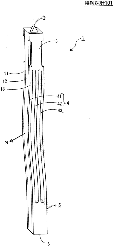
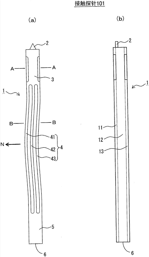
[0064] figure 1 as well as figure 2 It is an external view showing a configuration example of the contact probe 101 according to Embodiment 1 of the present invention. figure 1 is a perspective view of the contact probe 101, figure 2 (a) and (b) are side views respectively showing different side surfaces of the contact probe 101 . The contact probe 101 is a probe used for an electrical characteristic test of a semiconductor device, and is shown as an example of an electrical contact member.

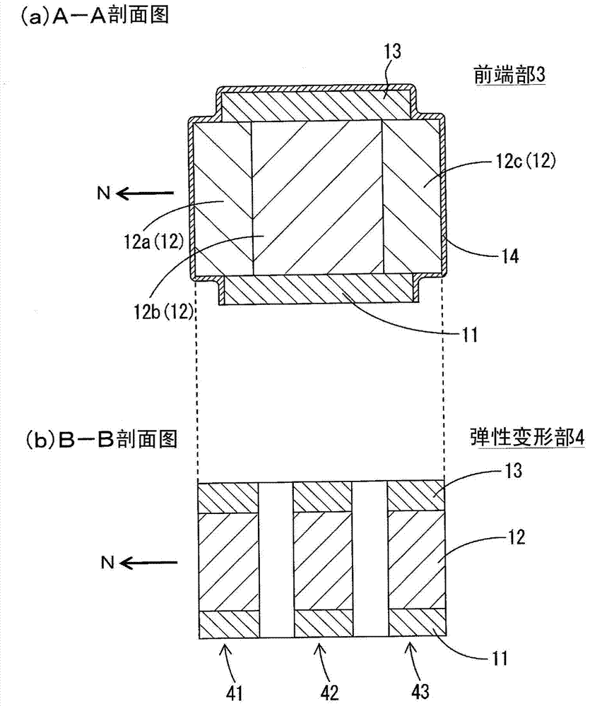
[0065] The above-mentioned contact probe 101 is a vertical type probe arranged vertically with respect to the object to be inspected, and includes: a substantially straight and elongated body portion 1; a contact portion 2 formed at the front end of the body portion 1; The terminal part 6 is provided at the root end. The main body 1 has a laminated structure composed of three metal layers 11 to 13 , and each metal layer 1 to 13 has a laminated surface extending along the longitudina...

Embodiment approach 2

[0113] In Embodiment 1, the contact probe 101 in which the tip portion 3 supported by the guide plate 120 has a cross-shaped cross section was described. On the other hand, in this embodiment, the contact probe 102 whose root part 5 supported by the guide plate 130 has a cross-shaped cross-section is demonstrated.

[0114] Figure 8 It is an external view showing an example of the configuration of the contact probe 102 according to Embodiment 2 of the present invention, and (a) and (b) in the figure respectively show different side surfaces of the contact probe 102 . Figure 9 yes means Figure 8 A cross-sectional view of an example of the configuration of the contact probe 102, showing that the Figure 8 The cross section when the root 5 is cut off by the C-C cutting line.

[0115] The contact probe 102 of this embodiment and the figure 2 Compared with the contact probe 101 (Embodiment 1), although the structure of the root portion 5 is different, other structures are th...

Embodiment approach 3

[0132] In Embodiments 1 and 2, an example in which the elastic deformation portion 4 is composed of the three beam portions 41 to 43 has been described. On the other hand, in this embodiment, the case where the elastic deformation part 4 is comprised by one beam part is demonstrated.

[0133] Figure 11 It is an external view showing a configuration example of the contact probe 103 according to Embodiment 3 of the present invention, and (a) and (b) in the figure respectively show different side surfaces of the contact probe 103 . If the contact probe 103 of this embodiment is combined with Figure 8 Compared with the contact probe 102 (Embodiment 2), although the structure of the elastic deformation part 4 is different, other structures are the same, and therefore, repeated descriptions are omitted.

[0134] The elastic deformation part 4 is constituted by one beam part formed of an elongated plate-shaped body, and a front end part 3 and a root part 5 are provided at both en...


PUM


Abstract

Provided is an electrical contact member that suppresses generation of chips caused by interference between a contact probe and a lead plate. It has a contact part (2), an elastic deformation part (4) and a front end part (3), and the contact part (2) has a laminated structure in which an intermediate metal layer (12) is sandwiched by outer metal layers (11, 13), And abutting against the object to be inspected, the elastic deformation part (4) is elastically deformed in a manner of bending in a predetermined bending direction (N) under the action of the compressive force in the longitudinal direction, and the front end part (3) is formed on the contact part (2) and the elastic deformation part (4), and is supported by the through hole (121) of the guide plate (120) so that the contact part (2) can move in the longitudinal direction, and the elastic deformation part (4) The side surface of the front end part (3) formed by the bending direction (N) and its opposite direction (N') is composed of three metal layers (11-13), and in this side surface, the metal layer (12) in the middle is larger than the metal layer on the outside. Layers (11, 13) are more prominent.

Description

technical field [0001] The present invention relates to an electrical contact member, and more specifically, to an electrical contact member in which a contact portion is brought into contact with an electrode terminal as the elastic deformation portion is elastically deformed, for example, it relates to an electrical contact member used in an electrical characteristic test of a semiconductor device. Improvements to contact probes. Background technique [0002] The electrical characteristic test of a semiconductor device is performed by bringing the semiconductor wafer close to a probe card with many contact probes formed on the wiring board, so that each contact probe is in contact with the electrode pad on the semiconductor wafer, and the test is performed via the contact probe signal input and output. [0003] When the contact probes are brought into contact with the electrode pads, the semiconductor wafer is further brought into contact with the probe card after the two...

Claims


Application Information

Patent Timeline
Patent Type & Authority Patents(China)
IPC IPC(8): G01R1/073H01L21/66
CPCG01R1/06716G01R1/07357G01R1/06738H01R13/2428
Inventor 木村哲平福岛则之浦田敦夫有田直树武田朋之
Owner NIHON DENSHIZAIRYO
Why Eureka
Try Eureka