Electrical contact
A technology of electrical contact and components, applied in the direction of electrical components, parts of connecting devices, circuits, etc., can solve the problems of decreased durability of contact probes, achieve the effects of inhibiting movement deterioration, preventing short circuits, and improving durability
- Summary
- Abstract
- Description
- Claims
- Application Information
AI Technical Summary
Problems solved by technology
Method used
Image

Examples
Embodiment approach 1
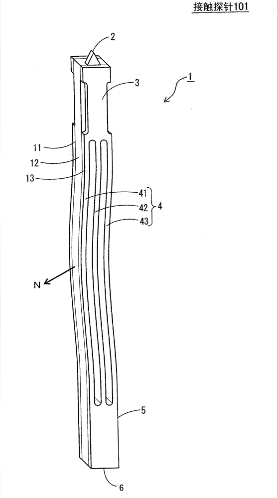
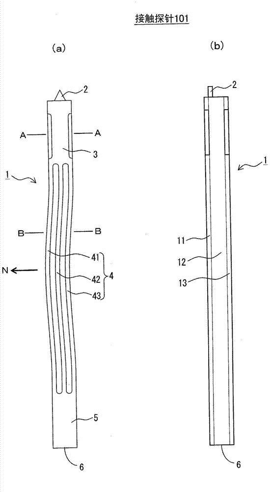
[0064] figure 1 as well as figure 2 It is an external view showing a configuration example of the contact probe 101 according to Embodiment 1 of the present invention. figure 1 is a perspective view of the contact probe 101, figure 2 (a) and (b) are side views respectively showing different side surfaces of the contact probe 101 . The contact probe 101 is a probe used for an electrical characteristic test of a semiconductor device, and is shown as an example of an electrical contact member.
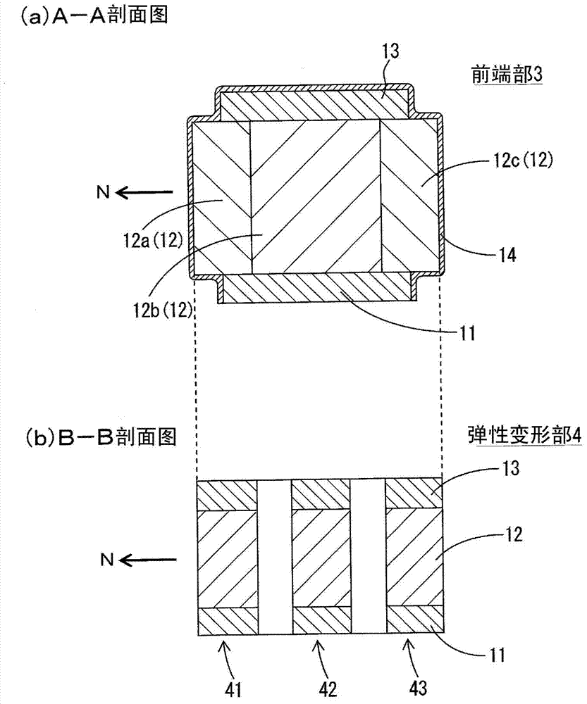
[0065] The above-mentioned contact probe 101 is a vertical type probe arranged vertically with respect to the object to be inspected, and includes: a substantially straight and elongated body portion 1; a contact portion 2 formed at the front end of the body portion 1; The terminal part 6 is provided at the root end. The main body 1 has a laminated structure composed of three metal layers 11 to 13 , and each metal layer 1 to 13 has a laminated surface extending along the longitudina...
Embodiment approach 2
[0113] In Embodiment 1, the contact probe 101 in which the tip portion 3 supported by the guide plate 120 has a cross-shaped cross section was described. On the other hand, in this embodiment, the contact probe 102 whose root part 5 supported by the guide plate 130 has a cross-shaped cross-section is demonstrated.
[0114] Figure 8 It is an external view showing an example of the configuration of the contact probe 102 according to Embodiment 2 of the present invention, and (a) and (b) in the figure respectively show different side surfaces of the contact probe 102 . Figure 9 yes means Figure 8 A cross-sectional view of an example of the configuration of the contact probe 102, showing that the Figure 8 The cross section when the root 5 is cut off by the C-C cutting line.
[0115] The contact probe 102 of this embodiment and the figure 2 Compared with the contact probe 101 (Embodiment 1), although the structure of the root portion 5 is different, other structures are th...
Embodiment approach 3
[0132] In Embodiments 1 and 2, an example in which the elastic deformation portion 4 is composed of the three beam portions 41 to 43 has been described. On the other hand, in this embodiment, the case where the elastic deformation part 4 is comprised by one beam part is demonstrated.
[0133] Figure 11 It is an external view showing a configuration example of the contact probe 103 according to Embodiment 3 of the present invention, and (a) and (b) in the figure respectively show different side surfaces of the contact probe 103 . If the contact probe 103 of this embodiment is combined with Figure 8 Compared with the contact probe 102 (Embodiment 2), although the structure of the elastic deformation part 4 is different, other structures are the same, and therefore, repeated descriptions are omitted.
[0134] The elastic deformation part 4 is constituted by one beam part formed of an elongated plate-shaped body, and a front end part 3 and a root part 5 are provided at both en...
PUM
| Property | Measurement | Unit |
|---|---|---|
| Length | aaaaa | aaaaa |
| Thickness | aaaaa | aaaaa |
| Thickness | aaaaa | aaaaa |
Abstract
Description
Claims
Application Information
PatSnap Eureka turns technology decisions into work you can execute. Powered by our Innovation Knowledge Graph, it runs expert workflows across engineering, life sciences, materials and intellectual property. Get your review-ready output in minutes.


