Manufacturing method of TFT (Thin Film Transistor) substrate structure

A production method and substrate technology, which are applied in the photoengraving process of the pattern surface, the original for photomechanical processing, the exposure device of the photoengraving process, etc. Complete and other problems, to avoid the slope of the groove becoming slower, the adhesion is not affected, and the display quality can be improved.

Active Publication Date: 2015-11-18
WUHAN CHINA STAR OPTOELECTRONICS TECH CO LTD
View PDF10 Cites 35 Cited by
  • Summary
  • Abstract
  • Description
  • Claims
  • Application Information

AI Technical Summary

Problems solved by technology

[0006] The flat layer 200 is usually a photosensitive material, such as image 3 As shown, using a photomask, a groove 210 can be formed on the planar layer 200 through an exposure and development process; after that, as Figure 4 As shown, an indium tin oxide (ITO) film 300 needs to be deposited on the planar layer 200 to be used as a common electrode (COM); since the common electrode is electrically insulated from the TFT, therefore, as Figure 5 As shown, it is necessary to coat a photoresist 400 (photoresist, PR) on the ITO film 300; after that, as Image 6 As shown, the photoresist 400 is exposed and developed, but because the thickness of the flat layer 200 is relatively large, generally about 2.5 μm, the slope (taper) of the groove 210 on the flat layer 200 is relatively steep, and when the photoresist is coated, The photoresist has high fluidity, and the photoresist at the taper corner is too thick, which will lead to incomplete exposure, resulting in photoresist residue at the taper corner in the trench 210; after that, if Figure 7 As shown, the ITO in the trench 210 of the planar layer not covered by the photoresist 400 is etched away, but because the photoresist remains at the taper corner position in the trench 210, ITO300' remains
[0007] However, ITO residues in the fan-out area 120s will cause a short circuit of the underlying metal lines, resulting in poor image quality such as abnormal images and split screens.
[0008] At present, the most commonly used method in the industry to improve ITO residues is to use buried trench and bridging technology, which is complicated in manufacturing process and high in cost.

Method used


Image

  • Manufacturing method of TFT (Thin Film Transistor) substrate structure
  • Manufacturing method of TFT (Thin Film Transistor) substrate structure
  • Manufacturing method of TFT (Thin Film Transistor) substrate structure

Examples


Embodiment Construction

[0041]In order to further illustrate the technical means adopted by the present invention and its effects, the following describes in detail in conjunction with preferred embodiments of the present invention and accompanying drawings.

[0042] see Figure 8 , the present invention provides a kind of manufacturing method of TFT substrate structure, comprises the following steps:

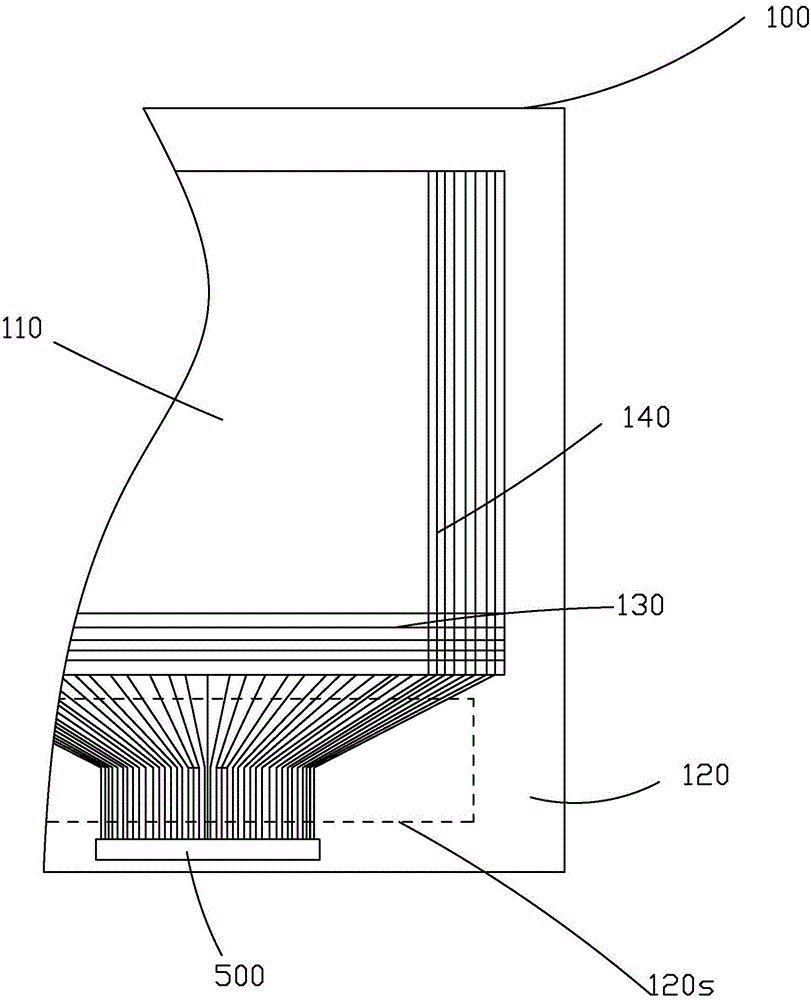
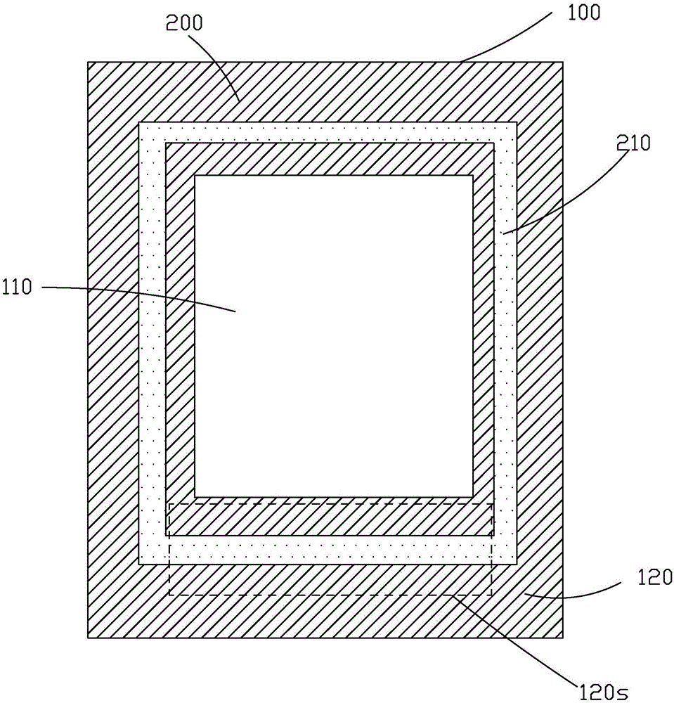
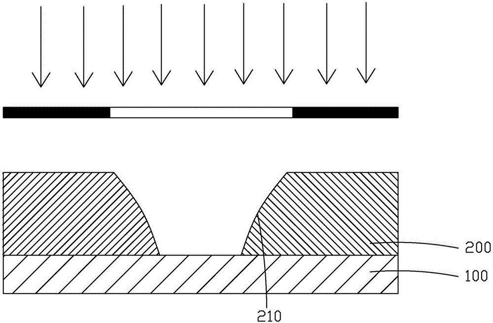
[0043] Step 1, such as Figure 9 As shown, a substrate 10 is provided, and a thin film transistor is arranged on the substrate 10; the substrate 10 includes an effective display area 11 and a peripheral circuit area 12 surrounding the effective display area 11, and the peripheral circuit area 12 includes a fan-out region 121 and the non-fan-out region; the planar layer 20 is formed by coating on the substrate 10 .

[0044] Specifically, the material of the flat layer 20 is organic photoresist.

[0045] Specifically, the thin film transistor is a low temperature polysilicon thin film transistor.

...


PUM

PropertyMeasurementUnit
thicknessaaaaaaaaaa

Abstract

The invention provides a manufacturing method of a TFT (Thin Film Transistor) substrate structure. According to the manufacturing method of the TFT substrate structure, via holes and a groove are formed in a planarization layer through single exposure by utilizing a halftone photomask, and half-exposure is realized through half-light-transmitting patterns on the halftone photomask; the groove with smaller depth is formed in the planarization layer of a fan-out area, so that the slope of the groove in the planarization layer of the fan-out area is decreased, the phenomenon of residue of a transparent conductive layer at corners of the groove caused by non-thorough photoresist exposure at the corners of the groove during photoresist exposure developing is avoided, and the phenomenon of short circuit between metal lines of the fan-out area is further avoided; meanwhile, the aperture ratio of an effective display area is not influenced, and the display quality of a liquid crystal display panel is greatly improved; moreover, by widening the groove in the planarization layer of the fan-out area, the phenomenon of reduction of an adhesion force of a frame sealing adhesive caused by decrease of the slope of the groove and reduction of the depth of the groove is avoided, and the adhesion property of the frame sealing adhesive in the liquid crystal display panel is further protected from being influenced.

Description

technical field [0001] The invention relates to the field of display technology, in particular to a method for manufacturing a TFT substrate structure. Background technique [0002] In the field of display technology, flat-panel displays such as Liquid Crystal Display (LCD) and Organic Light Emitting Diode (OLED) have gradually replaced CRT displays, and are widely used in LCD TVs, mobile phones, personal digital assistants, digital cameras, computer screens or laptop screen etc. [0003] Thin Film Transistor (TFT for short) is the main driving element in current liquid crystal display devices and active matrix driven organic electroluminescent display devices (ActiveMatrix / OrganicLight-EmittingDiode, AMOLED for short), and is directly related to the performance of high-performance flat panel display devices. Direction of development. Thin film transistors have various structures, and there are also various materials for preparing thin film transistors with corresponding s...

Claims


Application Information

Patent Timeline
Patent Type & Authority Applications(China)
IPC IPC(8): G03F1/32G03F7/20G02F1/1339
Inventor 史雷婷张占东
Owner WUHAN CHINA STAR OPTOELECTRONICS TECH CO LTD
Why Eureka
Try Eureka