Film transistor, array substrate, manufacturing method for array substrate, and display device

A technology of thin film transistor and manufacturing method, applied in the field of electronics, can solve the problems of increasing the power consumption of the display and the like

Inactive Publication Date: 2015-09-02
HEFEI XINSHENG OPTOELECTRONICS TECH CO LTD +1
View PDF4 Cites 3 Cited by
  • Summary
  • Abstract
  • Description
  • Claims
  • Application Information

AI Technical Summary

Problems solved by technology

However, when the channel width-to-length ratio of the TFT is greater than a certain threshold, the aperture ratio of the display (that is, the ratio of the effective light-transmitting area to the total area) will decrease accordingly, thereby increasing the energy consumption of the display.

Method used


Image

  • Film transistor, array substrate, manufacturing method for array substrate, and display device
  • Film transistor, array substrate, manufacturing method for array substrate, and display device
  • Film transistor, array substrate, manufacturing method for array substrate, and display device

Examples


Embodiment Construction

[0039] In the following description, for purposes of illustration rather than limitation, specific details, such as specific system architectures, interfaces, and techniques, are set forth in order to provide a thorough understanding of the present invention. It will be apparent, however, to one skilled in the art that the invention may be practiced in other embodiments without these specific details. In other instances, detailed descriptions of well-known devices, circuits, and methods are omitted so as not to obscure the description of the present invention with unnecessary detail.

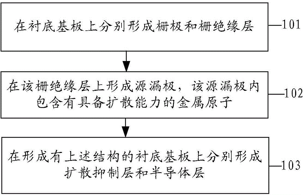
[0040] An embodiment of the present invention provides a manufacturing method of a thin film transistor, comprising: forming a source and a drain and a semiconductor layer on a base substrate.

[0041] Wherein, the source and drain electrodes contain metal atoms capable of diffusing; the material of the semiconductor layer is amorphous silicon.

[0042] Further, between the step of forming the ...


PUM


Abstract

The embodiment of the invention provides a film transistor, an array substrate, a manufacturing method for the array substrate, and a display device, and relates to the technical field of electronics. The ohmic contact resistance formed between an active layer and source-drain electrodes is reduced. The method comprises a step of forming a diffusion inhibition layer which is used for lowering the capability of diffusion of metal atoms in the source-drain electrodes to a semiconductor layer, wherein the step is operated between a step of forming the source-drain electrode and a step of forming a non-crystalline silicon semiconductor layer. The method also comprises a step of enabling the metal atoms diffused from the diffusion inhibition layer to react with amorphous silicon in a part, close to the source-drain electrode, of the semiconductor layer, and a step of generating a metal transition layer containing metal silicide. The method can be used for the manufacturing of the film transistor.

Description

technical field [0001] The invention relates to the field of electronic technology, in particular to a thin film transistor, an array substrate and a manufacturing method thereof, and a display device. Background technique [0002] In the field of liquid crystal display, the size of the TFT (Thin Film Transistor, Thin Film Transistor) on-state current (that is, the current value when a voltage is applied to the gate to turn on the active layer) is of great significance to the performance of the TFT, and the TFT on-state current The on-state resistance Ron is inversely proportional to the resistance value when the TFT is turned on. [0003] In the prior art, the back channel etching bottom gate structure is usually used to make the array substrate, and the on-state resistance of the TFT can be determined by figure 1 The model description shown, namely: [0004] Ron=2*R Ω +2*R V +R C , [0005] where Ron is the on-state resistance of the TFT, R Ω is the ohmic contact re...

Claims


Application Information

Patent Timeline
Patent Type & Authority Applications(China)
IPC IPC(8): H01L29/786H01L21/336H01L27/12
CPCH01L27/1214H01L29/6675H01L29/78663H01L29/458H01L29/66765H01L29/78618H01L29/78669H01L21/28518H01L29/0847H01L29/7845
Inventor 韩俊号尹炳坤马骏张敏
Owner HEFEI XINSHENG OPTOELECTRONICS TECH CO LTD
Why Eureka
Try Eureka