Trench MIS device having implanted drain-drift region and thick bottom oxide and process for manufacturing the same

A drift region and trench technology, applied in the manufacturing process of this MOSFET, in the field of trench gate power MOSFETs, can solve the problem of difficulty in reducing the on-state resistance of MOSFETs, achieve effective depletion, reduce on-state resistance, reduce Effect of on-state resistance

Active Publication Date: 2008-10-08
SILICONIX
View PDF4 Cites 0 Cited by
  • Summary
  • Abstract
  • Description
  • Claims
  • Application Information

AI Technical Summary

Problems solved by technology

Thus, using Bulucea's patented technology to improve the MOSFET's breakdown characteristics makes it more difficult to reduce the MOSFET's on-state resistance

Method used


Image

  • Trench MIS device having implanted drain-drift region and thick bottom oxide and process for manufacturing the same
  • Trench MIS device having implanted drain-drift region and thick bottom oxide and process for manufacturing the same
  • Trench MIS device having implanted drain-drift region and thick bottom oxide and process for manufacturing the same

Examples


Embodiment Construction

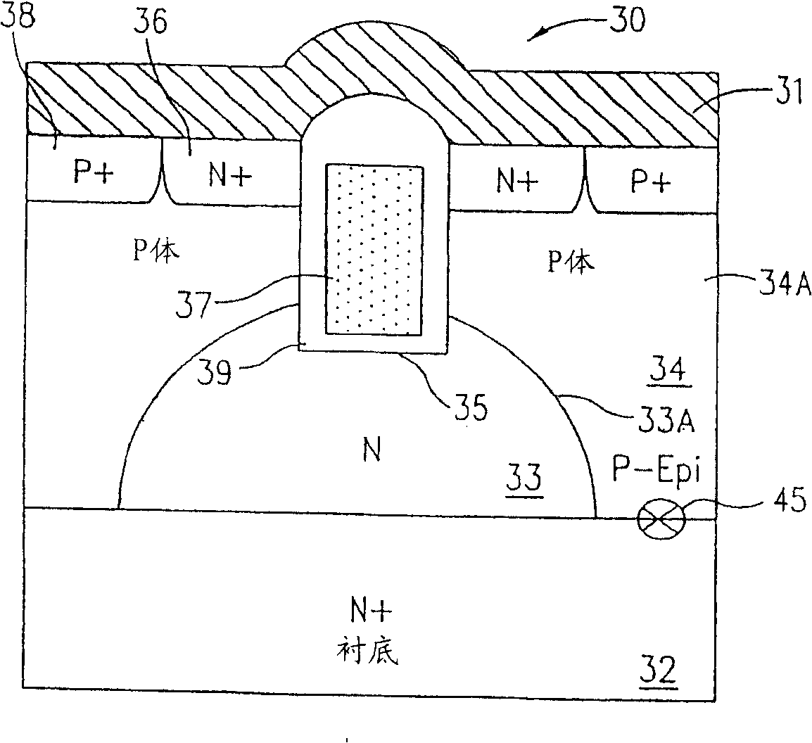
[0038] image 3 A cross-sectional view of a power MOSFET according to the invention is shown. MOSFET 30 is formed in N+ substrate 32 overlying epi layer 34, which is generally doped with P-type impurities (hereinafter simply referred to as P-epi layer 34). For example, N+ substrate 32 can have from 5×10 -4 ohm-cm to 5×10 -3 ohm-cm resistivity, P-epi layer 34 can be doped with from 1×10 15 cm -3 up to 5×10 17 cm -3 concentration of boron. N+ substrate 32 is typically about 200 microns thick, while epi layer 34 may be from 2 microns to 5 microns thick.

[0039] Trenches 35 are formed in P-epi layer 34 and trenches 35 contain polysilicon gates 37 . Gate 37 is electrically insulated from P-epi layer 34 by an oxide layer 39 extending along the sidewalls and bottom of trench 35 . MOSFET 30 also includes N+ source region 36 adjacent to the top surface of P-epi layer 34 and the sidewalls of trench 35 and P+ body contact region 38 . The remainder of the P-epi layer 34 forms a...


PUM


Abstract

A trench MOSFET is formed in a structure which includes a P-type epitaxial layer (100) overlying an N+ -type substrate (102). A trench is formed in the epitaxial layer (100). A deep implanted N-type layer (106) is formed below the trench at the interface between the substrate and the epitaxial layer, and N-type dopant is implant through the bottom of the trench to form an N-type region (120) in the epitaxial layer below the trench but above and separated from the deep N-type layer. The structure is heated to cause the N-type layer to diffuse upward and the N-type region to diffuse downward. The diffusions merge to form a continuous N-type drain-drift region (122) extending from the bottom of the trench to the substrate. Alternatively, the drain-drift region may be formed by implanting N-type dopant through the bottom of the trench at different energies, creating a stack of N-type regions that extend from the bottom of the trench to the substrate.

Description

[0001] This application is a CIP application of commonly owned Application No. 09 / 898,652 filed July 3, 2001, the entirety of which is incorporated herein by reference. technical field [0002] The invention relates to a power metal oxide semiconductor field effect transistor (MOSFET), in particular to a trench gate type power MOSFET with good on-state resistance and breakdown characteristics. The present application also relates to a process for manufacturing such a MOSFET. Background technique [0003] figure 1 A cross-sectional view of a conventional trench gate power MOSFET 10 is shown. MOSFET 10 is formed in N+ semiconductor substrate 11 on which N epitaxial layer 12 is grown. Gate 13 is formed in trench 14 extending downward from the top surface of N-epitaxial (N-epi) layer 12 . The gate is generally made of polysilicon and is electrically insulated from the N-epi layer 12 by an oxide layer 15 . A voltage applied to gate 13 controls current flow between N+ source r...

Claims


Application Information

Patent Timeline
Patent Type & Authority Patents(China)
IPC IPC(8): H01L29/78H01L21/336H01L29/08H01L21/225H01L29/06H01L29/10
CPCH01L21/2253H01L29/0847H01L29/1095H01L29/7813H01L29/0634H01L29/0878H01L29/7811H01L2924/0002H01L2924/00
Inventor 默罕穆德·N·达维什
Owner SILICONIX
Why Eureka
Try Eureka