Lateral double-diffused metal-oxide semiconductor field effect transistor and manufacturing method thereof

An oxide semiconductor and lateral double-diffusion technology, which is applied in semiconductor/solid-state device manufacturing, semiconductor devices, electrical components, etc., can solve the problem of small adjustable range of drift region and achieve high breakdown voltage and low on-state resistance Effect

Inactive Publication Date: 2012-07-11
SEMICON MFG INT (SHANGHAI) CORP
View PDF0 Cites 0 Cited by
  • Summary
  • Abstract
  • Description
  • Claims
  • Application Information

AI Technical Summary

Problems solved by technology

[0006] However, as the size of the device is getting smaller and smaller, the adjustable range of the drift region in LDMOS is getting smaller and smaller

Method used


Image

  • Lateral double-diffused metal-oxide semiconductor field effect transistor and manufacturing method thereof
  • Lateral double-diffused metal-oxide semiconductor field effect transistor and manufacturing method thereof
  • Lateral double-diffused metal-oxide semiconductor field effect transistor and manufacturing method thereof

Examples


Embodiment Construction

[0021] The implementation of the LDMOS and the method for fabricating the LDMOS of the present invention will be further described below in conjunction with the accompanying drawings and specific examples.

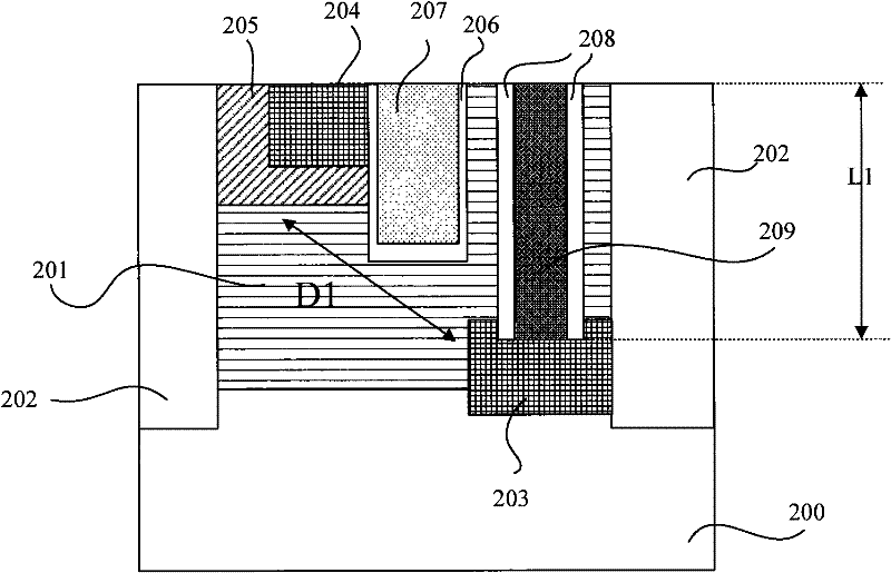
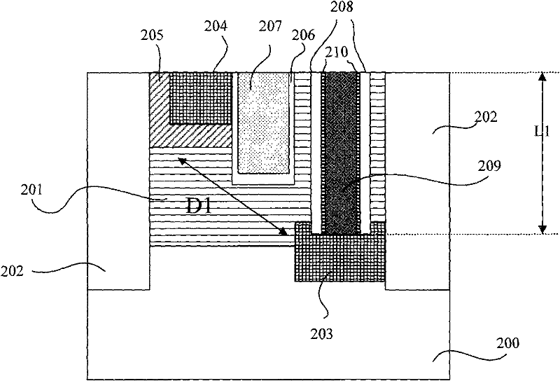
[0022] In a specific embodiment of the present invention, the provided LDMOS section diagram refers to figure 2 , the LDMOS may include: a substrate 200, a deep well 201 on the substrate 200 and isolation layers 202 on both sides; a gate insulating layer 206 located in the deep well 201, and a gate electrode 207 surrounded by the gate insulating layer 206; The first doped region 205 in the deep well on one side of the gate electrode 207, the second doped region 204 located in the first doped region, the first doped region 205 and the second doped region 204 and the gate insulating layer 206 Adjacent to: the contact hole 209 in the deep well on the other side of the gate electrode 207, and the drain 203 electrically connected to one end of the contact hole 209 in the deep ...


PUM


Abstract

The invention discloses a lateral double-diffused metal-oxide semiconductor field effect transistor and a manufacturing method thereof. The lateral double-diffused metal-oxide semiconductor field effect transistor comprises a substrate, deep trench on the substrate, insulating layers on the two sides of the deep trench, a grid structure in the deep trench, a source area which is positioned on thedeep trench beside the grid structure and has step-like current carrier concentration distribution, a contact hole positioned in the deep trench on the other side of the grid structure and a drain electrode connected with the end, which is in the deep trench, of the contact hole electrically, wherein there is a depth deference between the drain electrode and the source area. In the novel LDMOS element provided by the invention, the on resistance and the breakdown voltage can be regulated without increasing the lateral distance of the element.

Description

technical field [0001] The invention relates to a semiconductor device, especially a lateral double-diffused metal oxide semiconductor field effect transistor in a power semiconductor device and a manufacturing method thereof. Background technique [0002] Power field effect transistors mainly include two types: vertical double-diffused field effect transistor VDMOS (Vertical Double-Diffused MOSFET) and lateral double-diffused field effect transistor LDMOS (Lateral Double-Diffused MOSFET). Among them, compared with the vertical double diffused field effect transistor VDMOS, the lateral double diffused field effect transistor LDMOS has many advantages, for example, the latter has better thermal stability and frequency stability, higher gain and durability, lower Feedback capacitance and thermal resistance, as well as constant input impedance and simpler bias current circuit. [0003] On-state resistance (Rdson) and breakdown voltage BV (Breakdown Voltage) are two important p...

Claims


Application Information

Patent Timeline
Patent Type & Authority Patents(China)
IPC IPC(8): H01L29/78H01L29/06H01L21/336
Inventor 三重野文健
Owner SEMICON MFG INT (SHANGHAI) CORP
Why Eureka
Try Eureka