A method and device for writing data in nand FLASH

A technology for writing data and data, applied in the direction of memory address/allocation/relocation, etc., can solve problems such as writing or erasing operation errors, inability to erase and write infinitely, and limited life of NANDFLASH memory

Active Publication Date: 2018-04-13
HEFEI GEYI INTEGRATED CIRCUIT CO LTD +1
View PDF6 Cites 0 Cited by
  • Summary
  • Abstract
  • Description
  • Claims
  • Application Information

AI Technical Summary

Problems solved by technology

When writing or erasing bad blocks, it will cause errors in writing or erasing operations
In the application, the block skipping strategy is generally used to manage bad blocks, but it cannot solve the bad blocks generated during system operation
At the same time, the life of NAND FLASH memory is limited and cannot be erased and written indefinitely

Method used


Image

  • A method and device for writing data in nand FLASH
  • A method and device for writing data in nand FLASH
  • A method and device for writing data in nand FLASH

Examples


Embodiment Construction

[0081] In order to make the above objects, features and advantages of the present application more obvious and comprehensible, the present application will be further described in detail below in conjunction with the accompanying drawings and specific implementation methods.

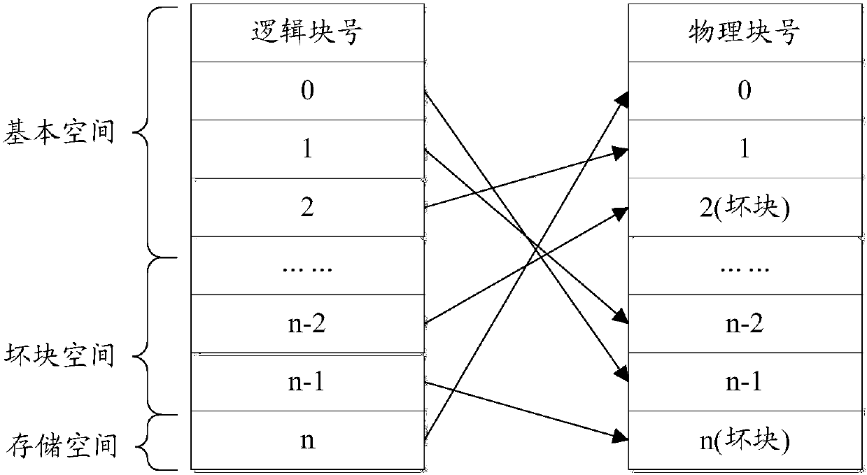
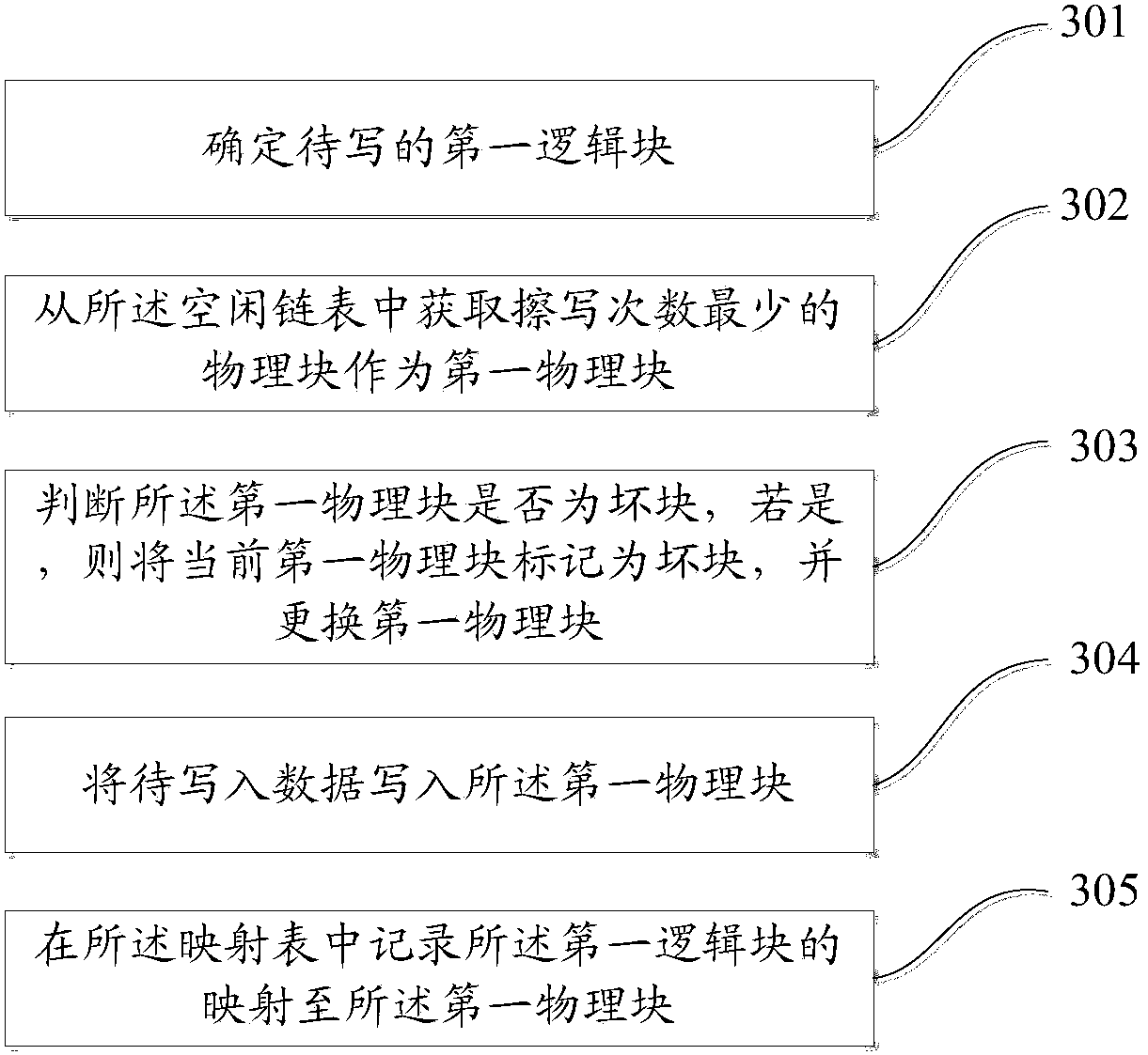
[0082] One of the core ideas of the embodiment of the present application is that during the write operation, the mapping of the logical address is converted to a physical block with the least number of erasures, so that the write operation is performed on a physical block with the least number of erasures of. At the same time, if it is found that the block to be written is a bad block, this block is added to the bad block space, and the block with the least number of erasures is found from the free list again to perform the write operation.

[0083] NAND FLASH is a kind of non-volatile flash memory. NAND FLASH is divided into several zones (regions), each zone is divided into several blocks (blocks), ea...


PUM


Abstract

The invention discloses a method for writing data in NAND FLASH, wherein NAND FLASH includes physical blocks, and the physical blocks have logical blocks mapped one by one, and the logical blocks include a mapping table and a free linked list, and the method includes: determining The first logical block to be written; Obtain the physical block with the least erasing times from the free linked list as the first physical block; judge whether the first physical block is a bad block, if so, mark the current first physical block is a bad block, and replace the first physical block; write the data to be written into the first physical block; record the mapping of the first logical block to the first physical block in the mapping table. This application uses the free linked list to achieve wear balance; the bad blocks found in the write operation are mapped to the bad block space, and the physical block with the least number of erasures is re-obtained from the free linked list for writing operations, so as to combine bad block management and wear balance.

Description

technical field [0001] The present application relates to the technical field of data storage, in particular to a method for writing data in NAND FLASH and a device for writing data in NAND FLASH. Background technique [0002] NAND FLASH is a non-volatile flash memory that can provide high capacity within a given chip size. It uses pages as the basic unit for storage and block as the basic unit for erasing. It has a very fast writing and erasing speed and is a better storage device than hard disk drives. [0003] While having many advantages, NAND FLASH may produce bad blocks during production and use due to problems in the production process, which will make the system unstable. When writing or erasing bad blocks, it will cause errors in writing or erasing operations. In applications, the block skipping strategy is generally used to manage bad blocks, but it cannot solve the bad blocks generated during system operation. At the same time, the life of NAND FLASH memory is ...

Claims


Application Information

Patent Timeline
Patent Type & Authority Patents(China)
IPC IPC(8): G06F12/06
Inventor 汤秋莲马斌王景华
Owner HEFEI GEYI INTEGRATED CIRCUIT CO LTD
Why Eureka
Try Eureka