A method and device for reading and writing data on a storage device

A storage device and data writing technology, which is applied in the field of information security and can solve problems such as affecting the service life of storage devices, damage to storage devices, and data loss of storage devices.

Active Publication Date: 2017-02-22
FEITIAN TECHNOLOGIES
View PDF4 Cites 0 Cited by
  • Summary
  • Abstract
  • Description
  • Claims
  • Application Information

AI Technical Summary

Problems solved by technology

[0002] With the development of science and technology, the market of smart cards continues to expand, and in the process of using smart cards, the smart card cannot work normally due to power failure, power failure or the quality of electricity not meeting the requirements under unknown circumstances. Erasing and writing operations on the storage device (that is, non-volatile storage area, including EEPROM, FLASH, etc.), will cause the loss of the original data in the storage device, greatly reducing the security of the smart card
[0003] In addition, when writing data to a storage device, data needs to be erased and written. In the actual process of erasing and writing, a certain page in the storage device is often erased and written frequently, so that the erase and write cannot be balanced. , and the erasing and writing life cycle of the storage device is generally 100,000 times. Due to excessive erasing and writing of some pages, the storage device will be damaged early, which seriously affects the service life of the storage device.

Method used


Image

  • A method and device for reading and writing data on a storage device
  • A method and device for reading and writing data on a storage device
  • A method and device for reading and writing data on a storage device

Examples


Embodiment 1

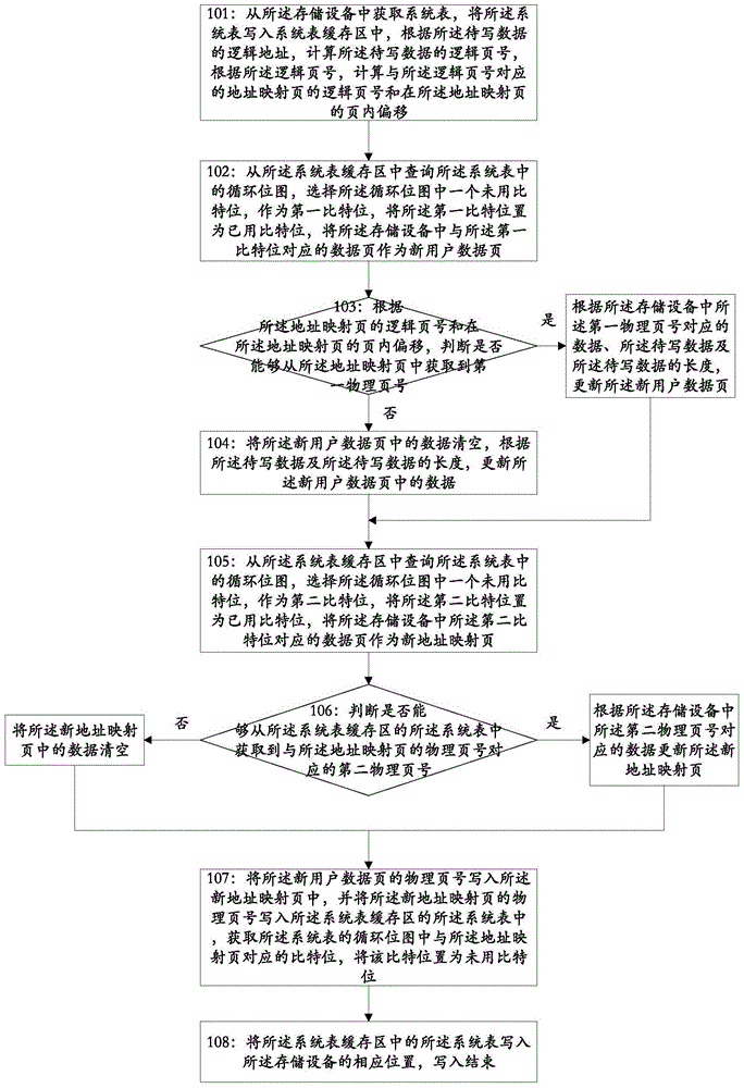
[0225] Embodiment 1 of the present invention provides a method for reading and writing data on a storage device, such as figure 1 As shown, it includes: calling the write function, passing the data to be written, the length of the data to be written, and the logical address of the data to be written to the write function, and the write function receives the incoming data to be written, After the length of the data to be written and the logical address of the data to be written, perform the following operations:

[0226] Step 101: Obtain a system table from the storage device, write the system table into the system table cache area, calculate the logical page number of the data to be written according to the logical address of the data to be written, and calculate the logical page number of the data to be written according to the A logical page number, calculating a logical page number of an address-mapped page corresponding to the logical page number and an offset within a pag...

Embodiment 2

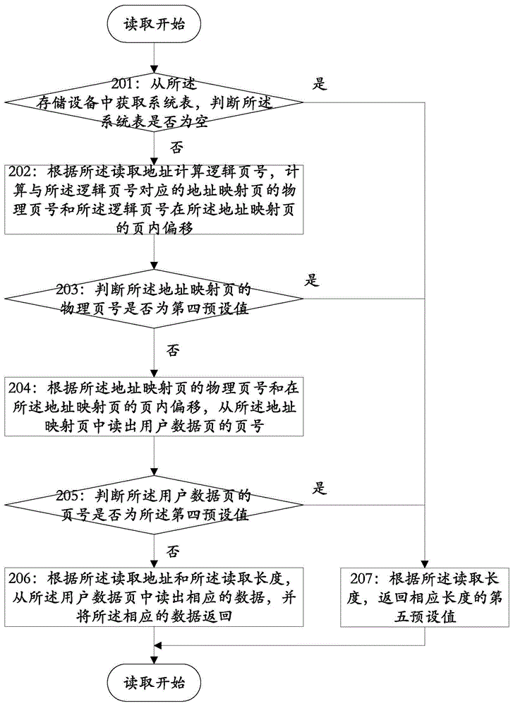
[0236] Embodiment 2 of the present invention provides a method for reading data from a storage device, such as figure 2 As shown, the storage device in this embodiment uses the method provided in Embodiment 1 to write data; the method includes: calling a read function, and passing in a read address (the address is a logical address) to the read function ) and read length, after the read function receives the incoming read address and read length, it performs the following operations:

[0237] Step 201: Acquiring a system table from the storage device, and judging whether the system table is empty, if yes, execute step 207, otherwise execute step 202;

[0238] Step 202: Calculate the logical page number according to the read address, calculate the physical page number of the address-mapped page corresponding to the logical page number and the offset of the logical page number within the page of the address-mapped page;

[0239] Step 203: judging whether the physical page numb...

Embodiment 3

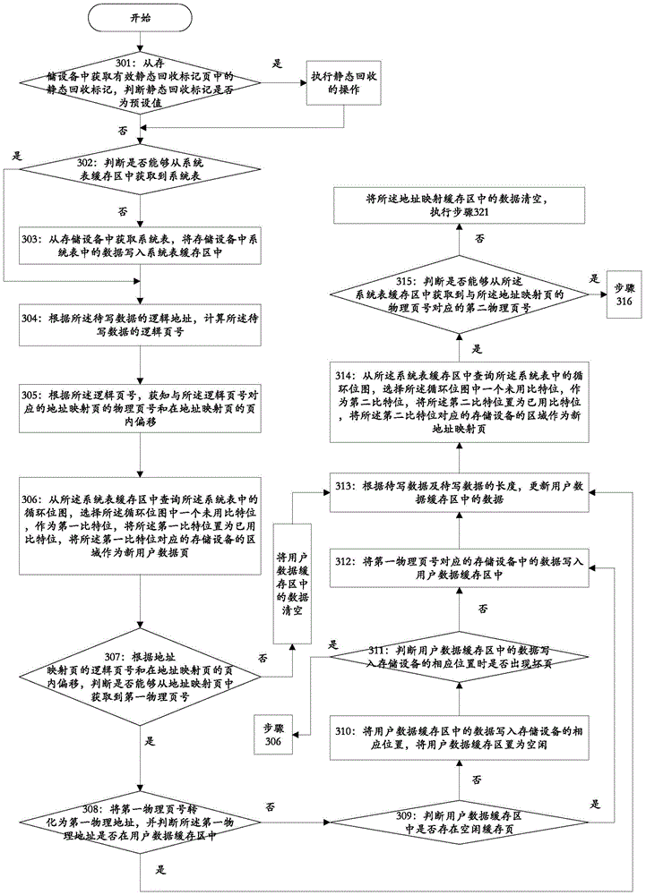
[0247] Embodiment 3 of the present invention provides a method for writing data to a storage device. In this embodiment, the preset page length is 256 bytes as an example for illustration, as shown in image 3 and Figure 4 As shown, it includes: calling the write function, passing the data to be written, the length of the data to be written, and the logical address of the data to be written to the write function, and the write function receives the incoming data to be written, After the length of the data to be written and the logical address of the data to be written, perform the following operations:

[0248] Step 301: Obtain the static recovery mark in the effective static recovery mark page from the storage device, judge whether the static recovery mark is a preset value, if yes, execute the operation of static recovery, and execute step 302, otherwise directly execute step 302;

[0249] Specifically, obtain the data in all the static recovery mark pages, obtain the valid ...


PUM


Abstract

The invention discloses a method and device for conducting data reading and writing on a storage device. The method for conducting data writing on the storage device comprises the steps that an unused bit of a circulation bitmap in a system table is selected, a new user data page and a new address mapping page are allocated, data to be written are written to the new user data page, a physical page number of the new user data page is written to the new address mapping page, the physical page number of the new address mapping page is written to the system table, and the system table is written to the storage device. The method for conducting data reading on the storage device comprises the steps that the physical page number of the address mapping page is obtained from the system table, the physical page number of the user data page is obtained from the address mapping page, and data needing to be read are obtained from the user data page. According to the technical scheme, data reading and writing are conducted according to the two-level mapping relation of the system table, the address mapping page and the user data page, power-down can be avoided through management of the circulation bitmap, the frequency for erasing the storage device is reduced through a cache mechanism, and abrasion balance is achieved.

Description

technical field [0001] The invention relates to the field of information security, in particular to a method and device for reading and writing data on a storage device. Background technique [0002] With the development of science and technology, the market of smart cards continues to expand, and in the process of using smart cards, the smart card cannot work normally due to power failure, power failure or the quality of electricity not meeting the requirements under unknown circumstances. Erasing and writing operations on the storage device (that is, the non-volatile storage area, including EEPROM, FLASH, etc.) will result in the loss of the original data in the storage device, greatly reducing the security of the smart card. [0003] In addition, when writing data to a storage device, data needs to be erased and written. In the actual process of erasing and writing, a certain page in the storage device is often erased and written frequently, so that the erase and write ca...

Claims


Application Information

Patent Timeline
Patent Type & Authority Patents(China)
IPC IPC(8): G06F3/06G06F12/16
Inventor 陆舟于华章
Owner FEITIAN TECHNOLOGIES
Why Eureka
Try Eureka