Structure and preparation method of a strained thin film
A strained film and pipeline technology, which is used in electric/magnetic solid deformation measurement, semiconductor/solid-state device manufacturing, electromagnetic measurement devices, etc. Pipeline maintenance cost, high sensitivity effect
- Summary
- Abstract
- Description
- Claims
- Application Information
AI Technical Summary
Problems solved by technology
Method used
Image
Examples
preparation example Construction
[0037] The preparation method of the strained film is as follows:
[0038] A. A channel is formed on the silicon substrate, and a plurality of piezoresistors are covered on the channel,
[0039]B. A plurality of piezoresistors are arranged in two rows and form a Wheatstone bridge arm.
[0040] C. The plurality of piezoresistors seal the channel to form a vacuum channel,
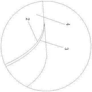
[0041] D. The part of the plurality of piezoresistors corresponding to the vacuum channel is a stress concentration area,
[0042] F, forming a drain region on a silicon substrate,
[0043] G. Forming a source region and a drift region on both sides of the channel on the silicon substrate, and setting a protective layer between the channel and the source region and the drift region.
[0044] The size of the strained film is width: 1-10cm, and the distance between two adjacent strained films is 10-20cm.
[0045] This embodiment also provides a method for testing ground network pipelines based on Beidou pos...
Embodiment 2
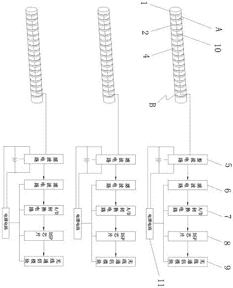
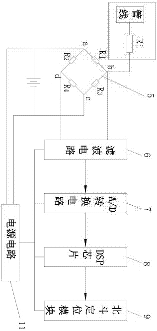
[0052] refer to Figure 4 As shown, this embodiment is basically the same as Embodiment 1, except that every n ring-shaped strained thin films 2 are connected in parallel through wires 10 to form a strained thin film group B. The equivalent circuit is also the same as that of the first embodiment. The equivalent resistance of the strained film group B is Ri, and this equivalent circuit is connected to the b terminal of the rectifier circuit 5. When the pipeline 1 is broken or slightly deformed, the corresponding annular strained film 2 is slightly deformed or broken, so that the strain The equivalent resistance Ri of the film group B changes. At this time, the resistance value is sent to the main control circuit 8 after the rectification circuit 5, the filter circuit 6, and the A / D conversion circuit 7. After monitoring the corresponding resistance value, it can be obtained The equivalent resistance of which strained film group B has changed, and the calculation result is sen...
PUM
 Abstract
Description
Claims
Application Information


