Method for manufacturing electric device and shielding member

A technology of electronic equipment and shielding parts, which is applied in the electronic field, can solve the problems of increasing the thickness and thickness of electronic equipment, and achieve the effect of preventing electromagnetic waves from radiating outward and preventing influence

Active Publication Date: 2015-08-05
HUAWEI DEVICE CO LTD
View PDF4 Cites 11 Cited by
  • Summary
  • Abstract
  • Description
  • Claims
  • Application Information

AI Technical Summary

Problems solved by technology

[0004] However, since the thickness of the metal die-casting itself is relatively thick, a conductive film is pasted on the hole or groove of the die-casting metal, which further increases the thickness of the electronic device.

Method used


Image

  • Method for manufacturing electric device and shielding member
  • Method for manufacturing electric device and shielding member
  • Method for manufacturing electric device and shielding member

Examples


Embodiment 1

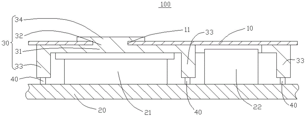
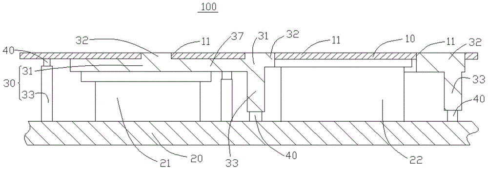
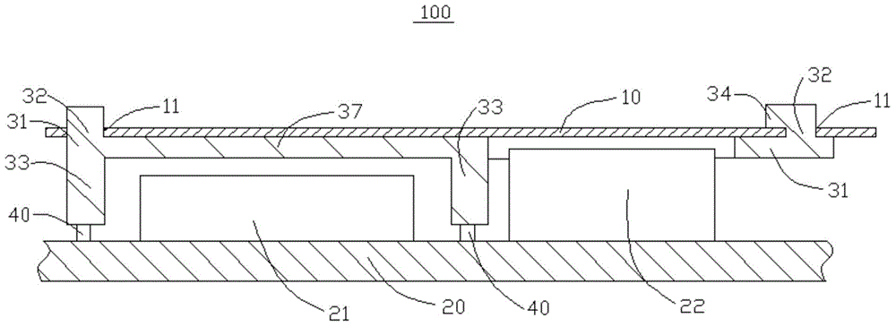
[0035] Such as figure 1 As shown, is a schematic structural diagram of an electronic device 100 according to an embodiment of the present invention. The electronic device can be mobile phone, PAD, computer, TV, server and other devices. The electronic device 100 includes a metal part 10 , a circuit board 20 and a shielding part 30 .

[0036] The metal piece 10 is provided with a through hole or a slot 11, and the shape and size of the hole or slot 11 can be set according to requirements. The function of opening the through hole or slot 11 is mainly to reduce the metal weight of the electronic device 100, or to release stress, or to make way for the electronic devices in the electronic device 100, or to be fixed on the metal part 10 for fixing. components. Therefore, as required, the number of said through holes or slots 11 can be one or more. Such as figure 1 As shown, the number of the through hole or slot 11 is one, and the purpose of opening the through hole or slot 11...

Embodiment 2

[0064] Based on the same inventive concept, the present application also provides a method for making a shield, such as Figure 7 As shown, it is a flow chart of the manufacturing method of the shielding member according to the embodiment of the present invention. Simultaneously combine figure 1 , the manufacturing method of the shielding member comprises the following steps:

[0065] Step 210, opening a through hole or a groove 11 on the metal part 10, the metal part 10 may be a metal stamping part or a metal forging part;

[0066] Step 220, forming a shielding part 31 on the metal part 10 by using a conductive plastic material through injection molding, and the shielding part 31 is used to shield the through hole or groove 11;

[0067] Step 230 , forming the enclosing portion 33 for enclosing the electronic device 21 on the circuit board 20 by metal or conductive plastic material.

[0068] Specifically, the method further includes: step 240, using plastic material to form...


PUM


Abstract

The embodiment discloses a method for manufacturing an electric device and a shielding member. The electric device includes a metal member, a circuit board and the shielding member. A through hole or a groove is opened on the metal member. The metal member is a metal punching member or a metal press forging member. The circuit board is arranged opposite to the metal member and is provided with electric devices. The shielding member is fixed on the metal member. The shielding member includes a blocking part and a sealing part. THe blocking part is made of conductive plastic materials. The sealing part is made of metal or conductive plastic materials. The blocking part is used for blocking the through hole or the groove. The sealing part surrounds the electric devices, and one end is electrically connected to the metal member, and the other end is electrically connected to the circuit board. The metal member, the blocking part, the shielding part and the circuit board form shielding space, and the electric devices are arranged in the shielding space.

Description

technical field [0001] The invention relates to the field of electronic technology, in particular to an electronic device and a manufacturing method of a shielding member. Background technique [0002] With the development of science and technology and the progress of society, electronic devices such as mobile phones, computers, and televisions have become an indispensable part of people's lives and work. Electronic equipment generally includes a circuit board on which electronic devices are installed and a die-cast metal part with holes or slots, wherein the die-cast metal part also serves as a shielding space for the electronic device. The purpose of opening the holes or slots is to reduce the weight of the die-cast metal parts, or due to the space constraints of the product structure and the layout of the devices, the holes or slots need to be opened (such as: the device is high, in order not to increase the overall thickness, the required Partial openings or grooves in ...

Claims


Application Information

Patent Timeline
Patent Type & Authority Applications(China)
IPC IPC(8): H05K9/00
CPCH05K9/0022G06F1/1656G06F1/182H05K9/0081B29C45/14639B29K2995/0005B29L2031/3481H05K9/0049
Inventor 靳林芳邹杰孙浩杨明星
Owner HUAWEI DEVICE CO LTD
Why Eureka
Try Eureka