An electronic device and a method for making the shield
A technology of electronic equipment and shielding parts, which is applied in the field of electronics, can solve the problems of thick thickness and increase the thickness of electronic equipment, and achieve the effect of preventing influence and avoiding the outward radiation of electromagnetic waves
- Summary
- Abstract
- Description
- Claims
- Application Information
AI Technical Summary
Problems solved by technology
Method used
Image
Examples
Embodiment 1
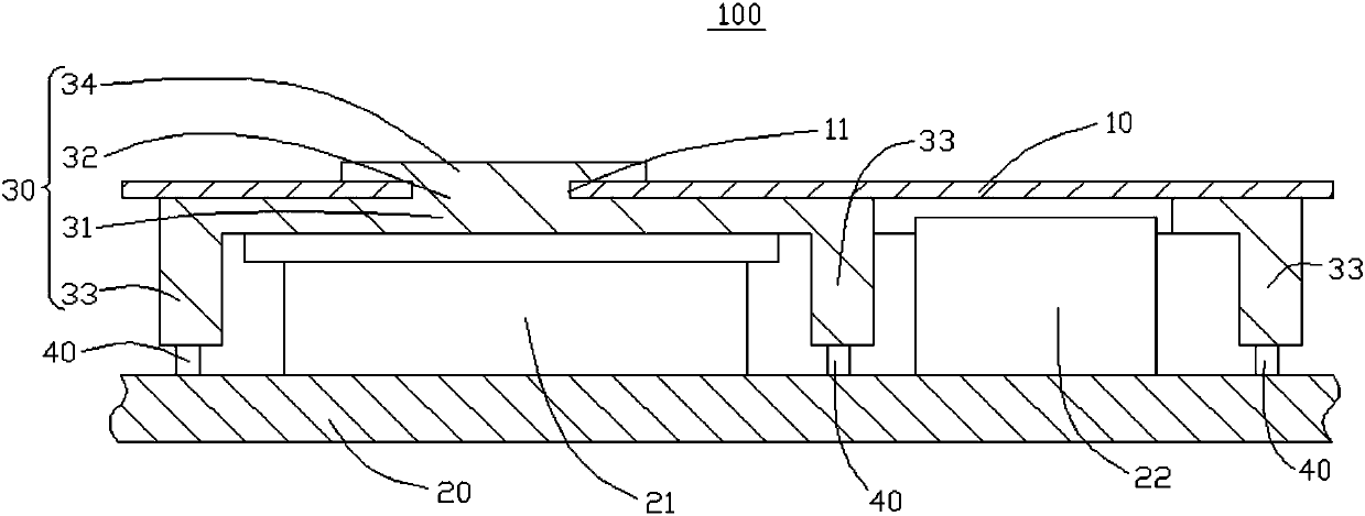
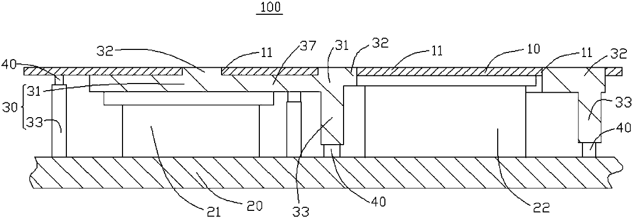
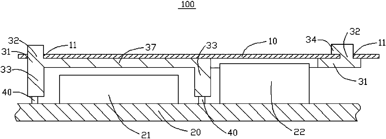
[0035] Such as figure 1 As shown, is a schematic structural diagram of an electronic device 100 according to an embodiment of the present invention. The electronic device can be mobile phone, PAD, computer, TV, server and other devices. The electronic device 100 includes a metal part 10 , a circuit board 20 and a shielding part 30 .
[0036] The metal piece 10 is provided with a through hole or a slot 11, and the shape and size of the hole or slot 11 can be set according to requirements. The function of opening the through hole or slot 11 is mainly to reduce the metal weight of the electronic device 100, or to release stress, or to make way for the electronic devices in the electronic device 100, or to be fixed on the metal part 10 for fixing. components. Therefore, as required, the number of said through holes or slots 11 can be one or more. Such as figure 1 As shown, the number of the through hole or slot 11 is one, and the purpose of opening the through hole or slot 11...
Embodiment 2
[0064] Based on the same inventive concept, the present application also provides a method for making a shield, such as Figure 7 As shown, it is a flow chart of the manufacturing method of the shielding member according to the embodiment of the present invention. Simultaneously combine figure 1 , the manufacturing method of the shielding member comprises the following steps:
[0065] Step 210, opening a through hole or a groove 11 on the metal part 10, the metal part 10 may be a metal stamping part or a metal forging part;
[0066] Step 220, forming a shielding part 31 on the metal part 10 by using a conductive plastic material through injection molding, and the shielding part 31 is used to shield the through hole or groove 11;
[0067] Step 230 , forming the enclosing portion 33 for enclosing the electronic device 21 on the circuit board 20 by metal or conductive plastic material.
[0068] Specifically, the method further includes: step 240, using plastic material to form...
PUM
 Abstract
Description
Claims
Application Information


