Liquid crystal display panel, liquid crystal display device and driving method of display device

A technology of liquid crystal display panel and liquid crystal display device, applied in static indicators, instruments, nonlinear optics, etc., can solve the problem of insufficient charging of pixel electrodes, and achieve the effects of stable display effect, increased charging time, and long charging time

Active Publication Date: 2015-08-19
WUHAN CHINA STAR OPTOELECTRONICS TECH CO LTD
View PDF4 Cites 36 Cited by
  • Summary
  • Abstract
  • Description
  • Claims
  • Application Information

AI Technical Summary

Problems solved by technology

[0005] The purpose of the present invention is to solve the defect of insufficient charging of the pixel electrodes in the prior art when the screen resolution increases

Method used


Image

  • Liquid crystal display panel, liquid crystal display device and driving method of display device
  • Liquid crystal display panel, liquid crystal display device and driving method of display device
  • Liquid crystal display panel, liquid crystal display device and driving method of display device

Examples


Embodiment 1

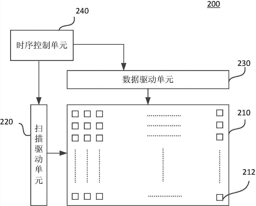
[0045] figure 2 is a schematic structural diagram of the liquid crystal display device 100 according to this embodiment. Such as figure 2 As shown, the liquid crystal display device 200 includes a display panel 210 , a scan driving unit 220 , a data driving unit 230 , and a timing control unit 240 . The display panel 210 includes a plurality of pixel units 212 arranged in an array.

[0046] The scan driving unit 220 and the data driving unit 230 are respectively electrically connected to the display panel 210 . The timing control unit 240 is electrically connected to the scan driving unit 220 and the data driving unit 230 for controlling the scan driving unit 220 to scan the display panel 210 and controlling the data driving unit 230 to drive the display panel 210 to display images.

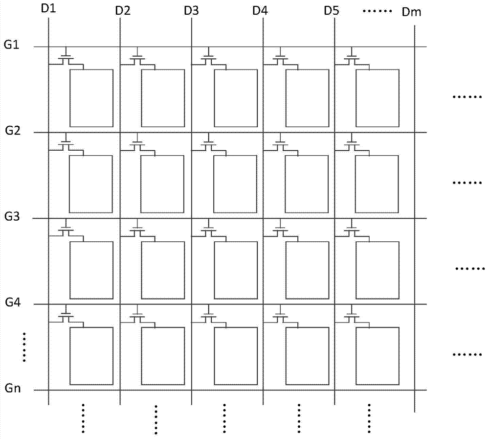
[0047] image 3 It is a schematic structural diagram of the display panel 210 according to this embodiment. In this embodiment, the display panel 210 includes multiple sets of data line pa...

Embodiment 2

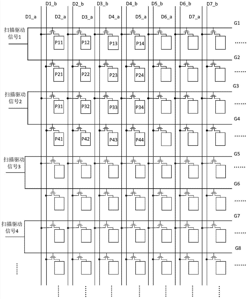
[0058] Figure 6 is a schematic structural diagram of a liquid crystal display panel according to this embodiment. The setting method of the data line is the same as that of the first embodiment, and will not be repeated here. The setting manner of the scanning lines is different from that in the first embodiment. exist Figure 6 , the first scan lines are G1, G2, G5, and G6, and the second scan lines are G3, G4, G7, and G8. There are two rows of pixel units between the first scanning line and the second scanning line, the two first scanning lines are adjacently arranged, and the two second scanning lines are adjacently arranged.

[0059] For the convenience of description, in this embodiment, two first pixel units arranged continuously in each column are defined as a "first pixel unit group". Similarly, two second pixel units arranged continuously in each column are defined as is the "second pixel unit group". Taking the first column of pixel units as an example, pixel u...

Embodiment 3

[0066] This embodiment provides a technical solution in which k rows of pixel units are separated between the first scan line and the second scan line. Figure 8 is a schematic structural diagram of a liquid crystal display panel according to this embodiment. The first scan lines are G1, G2, . . . , G(k), and the second scan lines are G(k+1), G(k+2), . . . , G(n). For ease of understanding, it is preferable to set n to be an even number in this example, and k=n / 2. exist Figure 8 Among them, the first scanning line and the second scanning line are separated by k rows of pixel units, the k first scanning lines are arranged adjacently, and the k second scanning lines are arranged adjacently.

[0067] Taking the first row of pixel units as an example, the pixel units P11 , P21 , . . . , Pk1 form a first pixel unit group, and P(k+1)1, . Then in the first column, the first pixel unit group and the second pixel unit group are alternately arranged, and the sources of the TFT switc...


PUM


Abstract

The invention discloses a liquid crystal display panel, a liquid crystal display device and a driving method of the liquid crystal display device. The liquid crystal display panel comprises multiple pairs of data lines, a plurality of scanning lines and a pixel unit array; the first scanning line and the second scanning line turn on TFT (thin film transistor) switches of two rows of pixel units at the same time according to scanning drive signals; the first data line and the second data line charge pixel electrodes of the two rows of pixel units through the TFT switches according to data drive signals. The charging time of the pixel electrodes is longer, and display effect is more stable. The liquid crystal display panel has more evident advantages when applied to high-definition display devices.

Description

technical field [0001] The invention relates to the technical field of liquid crystal display, in particular to a liquid crystal display panel, a display device and a driving method thereof. Background technique [0002] Existing liquid crystal display devices generally adopt a progressive scanning driving method to realize picture display. Such as figure 1 As shown, the liquid crystal display panel includes a plurality of pixel units defined by intersections of a plurality of scan lines (G1 to Gn) and a plurality of data lines (D1 to Dm), and each pixel unit includes a pixel electrode. When performing progressive scan driving, firstly provide scanning signals to the scanning lines G1 of the first row, the data lines charge the pixel electrodes of the first row, and then provide scanning signals to the scanning lines G2 of the second row, and the data lines charge the pixel electrodes of the first row. The pixel electrodes of the second row are charged, and so on. [0003...

Claims


Application Information

Patent Timeline
Patent Type & Authority Applications(China)
IPC IPC(8): G02F1/133G02F1/1362G02F1/1368
CPCG02F1/13306G02F1/136286G02F1/1368G09G2310/021G09G3/3648G09G2310/0251G09G3/36G02F2201/123G09G3/3677G09G3/3688G09G2300/0809
Inventor 邢振周左清成黄俊宏
Owner WUHAN CHINA STAR OPTOELECTRONICS TECH CO LTD
Why Eureka
Try Eureka