
Electroplating method and device for a circuit board

An electroplating device and circuit board technology, applied in the direction of electrolysis process, electrolysis components, cells, etc., can solve the problems of reduced production capacity, low efficiency, material waste, etc., and achieve the effect of improving production utilization and avoiding material waste

Active Publication Date: 2017-09-22
GCI SCI & TECH
View PDF20 Cites 2 Cited by
  • Summary
  • Abstract
  • Description
  • Claims
  • Application Information

AI Technical Summary

Problems solved by technology

[0004] However, the dummy board needs to be specially made for circuit boards with different material numbers, resulting in waste of materials and reduced production capacity. At the same time, for the production of small batches of circuit boards, the efficiency is low

Method used


Image

  • Electroplating method and device for a circuit board
  • Electroplating method and device for a circuit board
  • Electroplating method and device for a circuit board

Examples


Embodiment Construction

[0048] The following will clearly and completely describe the technical solutions in the embodiments of the present invention with reference to the accompanying drawings in the embodiments of the present invention. Obviously, the described embodiments are only some, not all, embodiments of the present invention. Based on the embodiments of the present invention, all other embodiments obtained by persons of ordinary skill in the art without creative efforts fall within the protection scope of the present invention.

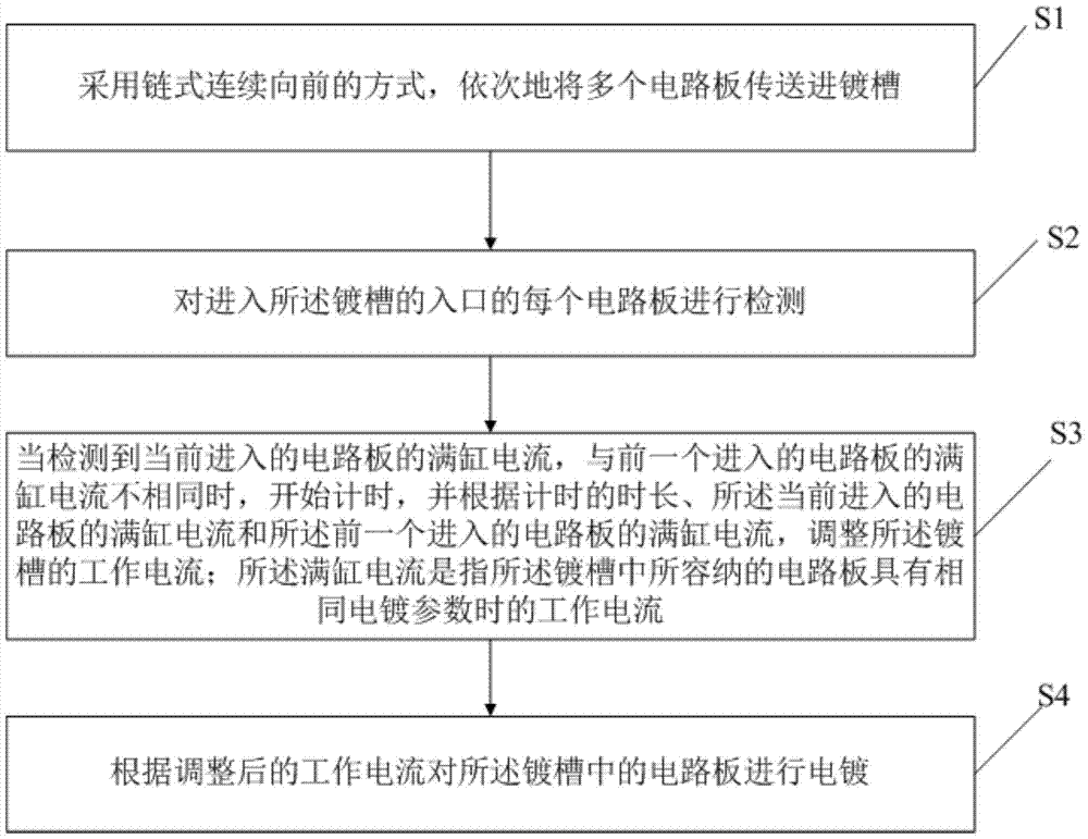
[0049] see figure 2 , is a schematic flow chart of an embodiment of an electroplating method for a circuit board provided by the present invention, including:

[0050] S1. Using the chain-type continuous forward method, multiple circuit boards are sequentially transported into the plating tank;

[0051] S2. Detect each circuit board entering the entrance of the plating tank;

[0052] S3. When it is detected that the full tank current of the current entering circ...


PUM


Abstract

The invention discloses an electroplating method for a circuit board, which comprises: sequentially transporting a plurality of circuit boards into a plating tank in a chain-type continuous forward manner; detecting each circuit board entering the entrance of the plating tank ; When it is detected that the full tank current of the current entering circuit board is different from the full tank current of the previous entering circuit board, start timing, and according to the length of timing, the full tank current of the currently entering circuit board and The full tank current of the circuit board entering the previous one adjusts the working current of the plating tank; the full tank current refers to the working current when the circuit boards accommodated in the plating tank have the same electroplating parameters; according to the adjustment The final working current is used to electroplate the circuit board in the plating tank. Correspondingly, the invention also discloses a circuit board electroplating device. By adopting the embodiment of the present invention, seamless switching of electroplating of different circuit boards can be realized, and the production utilization rate of circuit boards can be improved.

Description

technical field [0001] The invention relates to the technical field of circuit boards, in particular to an electroplating method and device for circuit boards. Background technique [0002] Continuous electroplating is an electroplating method in which the chain continuously conveys the circuit board forward to the plating tank for electroplating. Due to the different electroplating areas of circuit boards with different material numbers, the plating tank needs to use different working currents to electroplate circuit boards with different material numbers. In the prior art, for the continuous electroplating of circuit boards with different material numbers, it is generally used to add a dummy plate between two different material number circuit boards to realize the switching of the working current in the plating tank, wherein the length of the dummy plate and the length of the plating tank of the same length. [0003] Such as figure 1 As shown, the circuit board of mater...

Claims


Application Information

Patent Timeline
Patent Type & Authority Patents(China)
IPC IPC(8): C25D21/12C25D7/00
Inventor 詹世敬唐政和彭胜峰彭承刚
Owner GCI SCI & TECH
Learn More