Active matrix display panel with ground tie lines

A display panel, ground wire technology, used in static indicators, identification devices, instruments, etc.

Active Publication Date: 2015-08-26
APPLE INC
View PDF10 Cites 35 Cited by
  • Summary
  • Abstract
  • Description
  • Claims
  • Application Information

AI Technical Summary

Problems solved by technology

[0009] Although AMOLED display panels generally consume less power than liquid crystal display (LCD) panels, AMOLED display panels can still be the main power consumers in battery-operated devices

Method used


Image

  • Active matrix display panel with ground tie lines
  • Active matrix display panel with ground tie lines
  • Active matrix display panel with ground tie lines

Examples


Embodiment Construction

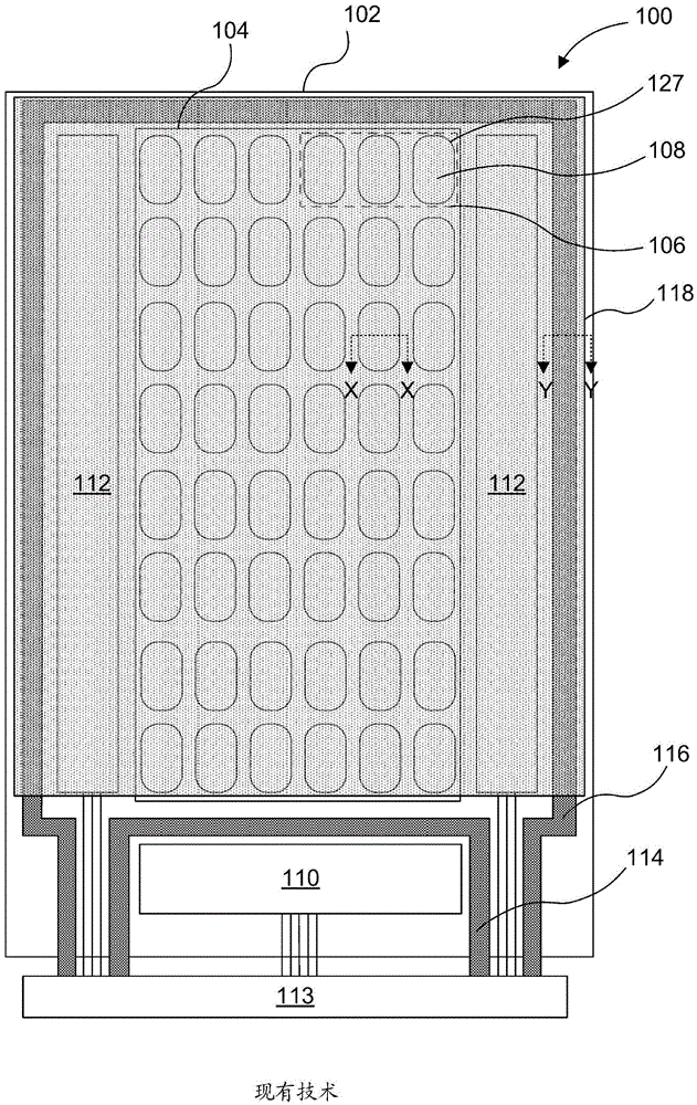
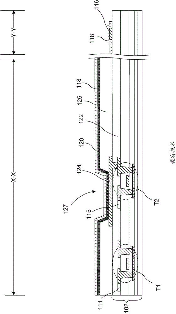
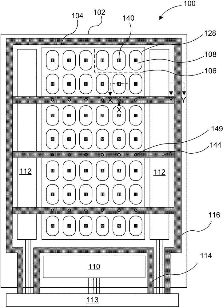
[0036] Embodiments of the invention relate to display systems. More specifically, embodiments of the present invention relate to ground structures for active matrix display panels.

[0037] In one embodiment, an active matrix display panel comprises an arrangement of ground connection lines extending between bank openings in pixel regions of the display panel. A top electrode layer may be deposited over all LEDs within the bank opening and be in electrical contact with the ground bond, or separate multiple top electrode layers may be deposited over one or more LEDs within the bank opening and be in contact with one or more LEDs within the bank opening. A plurality of ground bonds are in electrical contact. In one aspect, the arrangement of the ground bond lines can more evenly distribute the ground signal to the LED arrays on the display panel, thereby providing more uniform light emission across the panel. On the other hand, the arrangement of the ground bonding wires makes...


PUM


Abstract

A display panel and a method of forming a display panel are described. The display panel may include a thin film transistor substrate including a pixel area and a non-pixel area. The pixel area includes an array of bank openings and an array of bottom electrodes within the array of bank openings. A ground line is located in the non-pixel area and an array of ground tie lines run between the bank openings in the pixel area and are electrically connected to the ground line in the non-pixel area.

Description

[0001] Related Patent Applications [0002] This patent application is a continuation-in-part of US Patent Application No. 13 / 710,443 filed December 10, 2012, which is incorporated herein by reference. technical field [0003] Embodiments of the invention relate to display systems. More specifically, embodiments of the present invention relate to ground structures for active matrix display panels. Background technique [0004] Flat panel displays are becoming increasingly popular in a wide variety of electronic devices. Common types of flat panel displays include active matrix displays and passive matrix displays. Each pixel in an active-matrix display panel is driven by an active driver circuit, while each pixel in a passive-matrix display panel does not use such a driver circuit. High resolution color display panels such as modern computer monitors, smartphones and televisions typically use an active matrix display panel structure for better image quality. [0005] One...

Claims


Application Information

Patent Timeline
Patent Type & Authority Applications(China)
IPC IPC(8): G09F9/30
CPCH01L25/0753H01L2924/0002H01L33/20H01L27/156H01L24/95H01L33/42G09G3/32H01L27/124H01L2924/12044H01L2924/12041H01L2924/12042H01L2924/00H01L33/62
Inventor K·V·萨卡里亚A·比布尔胡馨华
Owner APPLE INC
Why Eureka
Try Eureka