Phase change memory element and manufacturing method thereof

A manufacturing method and phase change technology, applied in the direction of electrical components, etc., can solve the problems of insufficient conversion, slow heating and cooling speed, large current flow, etc.

Active Publication Date: 2015-09-09
北京时代全芯存储技术股份有限公司 +2
View PDF7 Cites 3 Cited by
  • Summary
  • Abstract
  • Description
  • Claims
  • Application Information

AI Technical Summary

Problems solved by technology

It is known that the heater of the phase change memory element has a large contact area with the memory element coupled to it. In addition to the common defects of surface holes, the large contact area also slows the heating and cooling speed (high resistance value The conversion between low resistance and low resistance is not fast enough, and the amount of current required is relatively large

Method used


Image

  • Phase change memory element and manufacturing method thereof
  • Phase change memory element and manufacturing method thereof
  • Phase change memory element and manufacturing method thereof

Examples


Embodiment Construction

[0023] In order to make the description of the present invention more detailed and complete, the following provides an illustrative description of the implementation modes and specific examples of the present invention; but this is not the only form for implementing or using the specific embodiments of the present invention. The various embodiments disclosed below can be combined or replaced with each other when beneficial, and other embodiments can also be added to one embodiment, without further description or illustration. In the following description, numerous specific details will be set forth in order to enable readers to fully understand the following embodiments. However, embodiments of the invention may be practiced without these specific details.

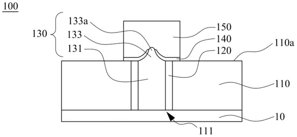
[0024] Please refer to Figure 1A . Figure 1A is a cross-sectional view of a phase change memory device 100 according to an embodiment of the present invention. The phase change memory device includes a substrate 10 , ...


PUM


Abstract

The invention related to a phase change memory element and a manufacturing method thereof. The phase change memory element comprises a dielectric layer, a metal barrier layer, a heater, an insulating layer, and a phase change layer. The dielectric layer has a surface and a channel which runs through the dielectric layer. The metal barrier layer serves as the lining of the channel. The heater is arranged in the channel and includes a needle-shaped part and a cylindrical part, and the needle-shaped part protrudes from the surface of the dielectric layer. The insulating layer is arranged on the surface of the dielectric layer, and covers part of the heater. The phase change layer is arranged on the surface of the dielectric layer, and contacts the needle-shaped part of the heater. According to the method of the invention, the contact area between the heater and a memory is changed to achieve high current density so as to improve the heat conversion efficiency of the heater.

Description

technical field [0001] The invention relates to a memory element and its manufacturing method, especially a phase-change memory element. Background technique [0002] Electronics (e.g. cell phones, tablets, and digital cameras. > Often have memory elements that store data. It is known that memory devices can store information through storage nodes on the memory unit. Among them, the phase change memory utilizes the resistance state (such as high resistance value and low resistance value) of the memory element to store information. A memory device may have a material that can change between different phases (eg, crystalline and amorphous) when programmed. The different phases of the materials cause the memory cells to have different resistance states with different resistance values, which represent different values ​​of stored data. [0003] When a phase-change memory cell is programmed, an electric current can be applied to heat the memory element to a certain temper...

Claims


Application Information

Patent Timeline
Patent Type & Authority Applications(China)
IPC IPC(8): H01L45/00
Inventor 吴孝哲王博文
Owner 北京时代全芯存储技术股份有限公司
Why Eureka
Try Eureka