Display panel and driving method thereof

A display panel and data driver technology, applied in the liquid crystal field, can solve problems such as display panel startup flickering, and achieve the effect of avoiding flickering

Active Publication Date: 2015-09-16
TCL CHINA STAR OPTOELECTRONICS TECH CO LTD
View PDF8 Cites 26 Cited by
  • Summary
  • Abstract
  • Description
  • Claims
  • Application Information

AI Technical Summary

Problems solved by technology

[0004] The technical problem mainly solved by the present invention is to provide a display panel and its driving method, which can solve the problem of flickering when the display panel is turned on due to wrong power sequence

Method used


Image

  • Display panel and driving method thereof
  • Display panel and driving method thereof
  • Display panel and driving method thereof

Examples


Embodiment Construction

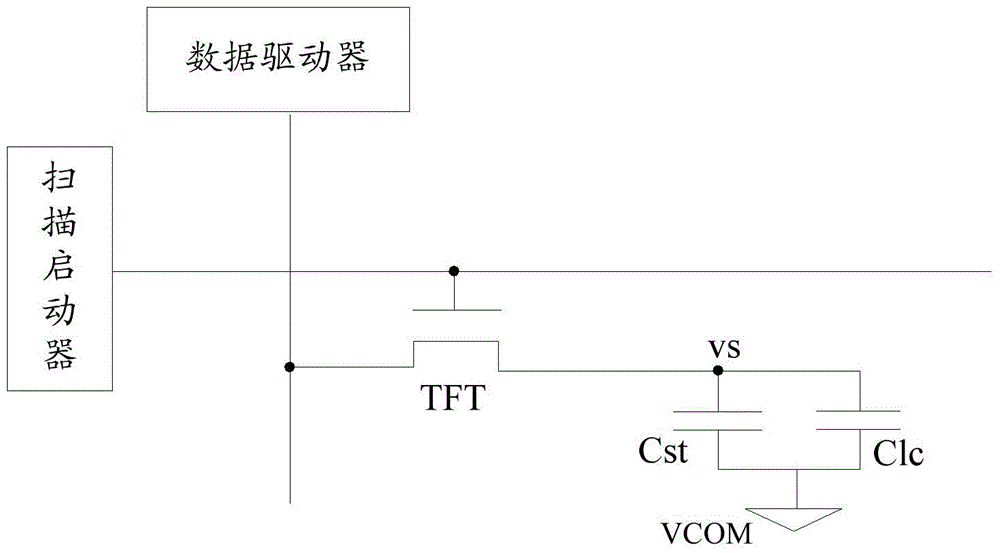
[0023] The invention discloses a display device, which includes a display panel, such as Figure 4-Figure 5 As shown, the display panel includes an array substrate 11 , a data driver 12 , a scan driver 13 and a control switch 14 . In this embodiment, the control switch 14 is independently arranged in the display panel. It should be understood that, in other embodiments, the control switch 14 can be set in the data driver 12 , which is a part of the data driver 12 , and the control switch 14 can be controlled by the data driver 12 . Alternatively, the control switch 14 is set in a timing controller (not shown), and the control switch 14 can be controlled by the timing controller.

[0024] The data driver 12 is used for providing data signals to the array substrate 11 to drive the array substrate 11 .

[0025] The scan driver 13 is used to provide scan signals for the array substrate to perform signal scanning on the array substrate 11 .

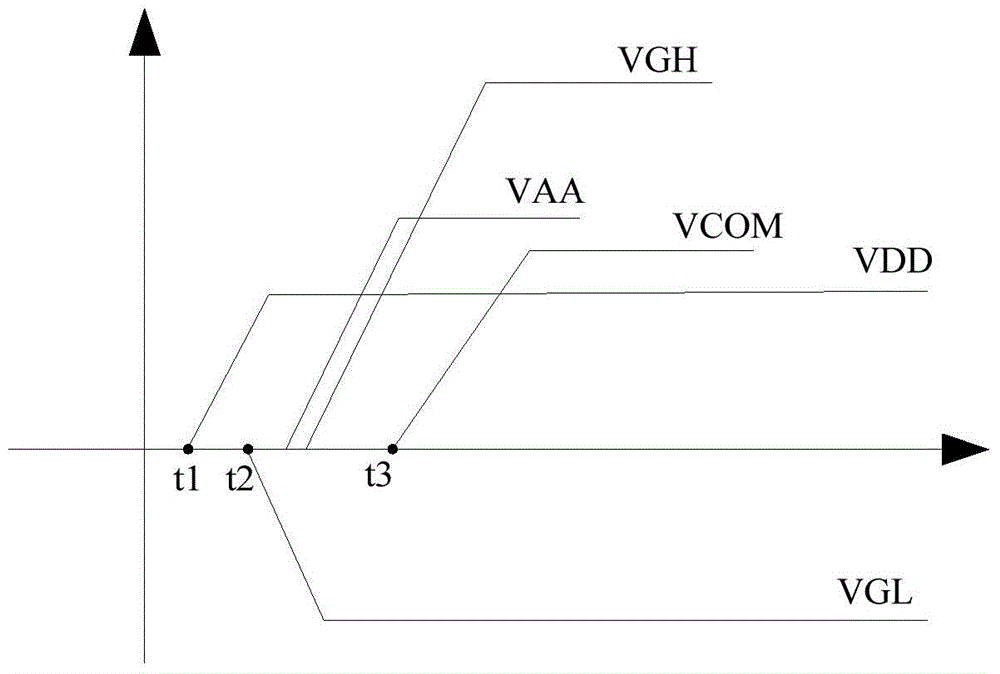
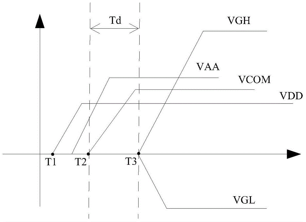
[0026] The control switch 14 is used...


PUM


Abstract

The invention discloses a display panel driving method. The display panel comprises an array substrate and a data driver, wherein the array substrate comprises a pixel unit, a common electrode line, a data line and a scanning line, wherein the pixel unit is respectively connected with the common electrode line, the data line and the scanning line; and the data driver is connected with the pixel unit via the data line. The method comprises steps: when the display panel starts initialization, the pixel unit and the data driver are controlled to be disconnected; after the display panel completes initialization, the pixel unit and the data driver are controlled to be connected so as to enable the data driver to provide data signals to drive the display panel. The invention also discloses the display panel. Through the above mode, through disconnecting the pixel unit and the data driver when the display panel is initialized, a splash screen phenomenon of the display panel at the moment of start-up can be prevented.

Description

technical field [0001] The invention relates to the field of liquid crystal technology, in particular to a display panel and a driving method thereof. Background technique [0002] In the traditional display panel driving process, in the normal power supply timing diagram of the display panel startup, the data driver starts the off-end voltage VGL of the thin film transistor before the power supply of the common electrode wiring VCOM starts, that is, at time t2, the data driver starts The off-end voltage VGL of the thin film transistor, and then start the power supply of the common electrode wiring VCOM at t3 ( figure 2 shown), in this case the display panel displays normally. If the timing of the off-end voltage VGL of the thin film transistor and the power supply of the common electrode line VCOM is wrong at the moment when the display panel is turned on, the power supply of the off-end voltage VGL of the thin film transistor activated by the data driver is started later ...

Claims


Application Information

Patent Timeline
Patent Type & Authority Applications(China)
IPC IPC(8): G09G3/36G02F1/133
CPCG09G3/3648G09G3/3688G09G2320/0247G09G2330/026
Inventor 吴晶晶郭东胜
Owner TCL CHINA STAR OPTOELECTRONICS TECH CO LTD
Why Eureka
Try Eureka