Array substrate and manufacturing method thereof, touch control display panel and touch control display apparatus

A touch display panel and array substrate technology, which is applied in semiconductor/solid-state device manufacturing, instruments, semiconductor devices, etc., can solve problems such as black lines, achieve the effects of improving quality, improving product yield, and reducing production costs

Active Publication Date: 2015-09-23
SHANGHAI TIANMA MICRO ELECTRONICS CO LTD +1
View PDF5 Cites 12 Cited by
  • Summary
  • Abstract
  • Description
  • Claims
  • Application Information

AI Technical Summary

Problems solved by technology

[0005] Embodiments of the present invention provide an array substrate and a manufacturing method, a touch display panel, and a touch display device, which s...

Method used


Image

  • Array substrate and manufacturing method thereof, touch control display panel and touch control display apparatus
  • Array substrate and manufacturing method thereof, touch control display panel and touch control display apparatus
  • Array substrate and manufacturing method thereof, touch control display panel and touch control display apparatus

Examples


Embodiment Construction

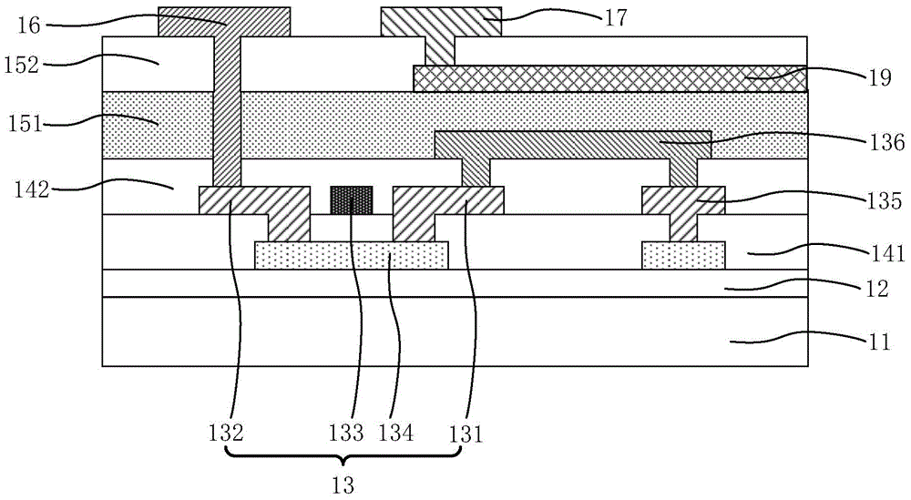
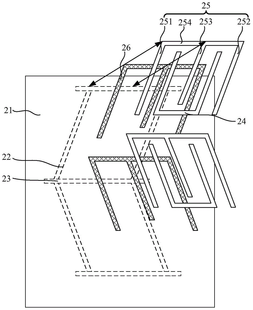
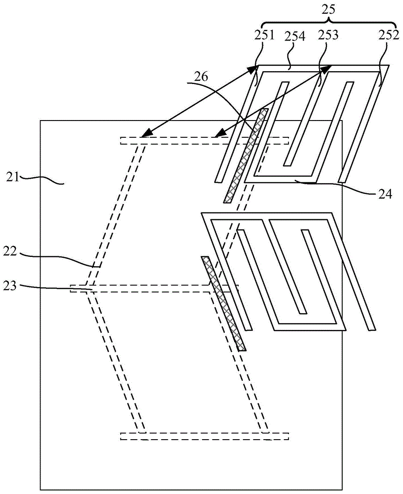
[0023] The present invention will be further described in detail below in conjunction with the accompanying drawings and embodiments. It should be understood that the specific embodiments described here are only used to explain the present invention, but not to limit the present invention. In addition, it should be noted that, for the convenience of description, only the parts related to the present invention are shown in the drawings but not the whole content.

[0024] The embodiment of the present invention integrates the touch function on the basis of the IPS (In-Plane Switching, in-plane switching) display mode. IPS display mode is a display technology in which liquid crystal molecules rotate in a plane to achieve brightness control. It has the advantages of excellent viewing angle characteristics, high dynamic definition and good color reproduction effect. The characteristic of the IPS display mode display is that the pixel electrodes and the common electrodes are arran...


PUM


Abstract

The present invention discloses an array substrate and a manufacturing method thereof, a touch control display panel and a touch control display apparatus. The array substrate comprises: a substrate; a plurality of data lines and a plurality of scanning lines, the plurality of data lines and the plurality of scanning lines being insulated and intersected to define a plurality of pixel units; a pixel electrode arranged in each of the plurality of pixel units; a common electrode arranged in the same layer as the pixel electrode, the common electrode comprising a plurality of common electrode blocks; and a plurality of touch sensing lines arranged between the membranous layer of the common electrode and the data lines, the touch sensing line being electrically connected to a corresponding common electrode block and being insulated from the common electrode blocks except the corresponding common electrode block, and at least one of the touch sensing lines being integrally or partially overlapped with the common electrode blocks. According to the present invention, black lines in the position where the touch sensing lines are arranged can be prevented, thereby improving the quality of displayed images.

Description

technical field [0001] The present invention relates to the field of display technology, in particular to an array substrate and a manufacturing method, a touch display panel and a touch display device. Background technique [0002] With the rapid development of display technology, touch screens have gradually pervaded people's lives. Compared with the traditional display which can only provide the display function, the display using the touch screen can enable information interaction between the user and the display control host. Therefore, the touch screen can completely or at least partially replace the common input device. A touch-enabled display can not only display, but also be controlled via an internal touch unit. [0003] Common touch screens are mainly divided into resistive touch screens, capacitive touch screens, electromagnetic touch screens and infrared blocking touch screens. In the existing electromagnetic touch screen, generally, the liquid crystal display...

Claims


Application Information

Patent Timeline
IPC IPC(8): G06F3/046G06F3/041H01L27/12H01L21/77
CPCG06F3/041G06F3/046H01L27/1214H01L27/124
Inventor 于泉鹏袁永魏丹萍
Owner SHANGHAI TIANMA MICRO ELECTRONICS CO LTD
Why Eureka
Try Eureka