
Active element array substrate

An array substrate and active component technology, applied in the field of active component array substrates, can solve problems such as resistive and capacitive loads, large height differences, etc., and achieve the effect of avoiding electrical problems

Inactive Publication Date: 2018-02-09
AU OPTRONICS CORP
View PDF4 Cites 0 Cited by
  • Summary
  • Abstract
  • Description
  • Claims
  • Application Information

AI Technical Summary

Problems solved by technology

However, due to the large height difference between the trench and the flat layer, there may be metal residues at the junction of the flat layer and the trench in the subsequent manufacturing process, and these residual metals may be mixed with other Electronic circuits generate electrical coupling, which in turn causes problems with resistive and capacitive loads

Method used


Image

  • Active element array substrate
  • Active element array substrate
  • Active element array substrate

Examples


Embodiment Construction

[0074] A number of embodiments of the present invention will be disclosed in the following figures. For the sake of clarity, many practical details will be described together in the following description. It should be understood, however, that these practical details should not be used to limit the invention. That is, in some embodiments of the present invention, these practical details are unnecessary. In addition, for the sake of simplifying the drawings, some existing conventional structures and elements will be shown in a simple and schematic manner in the drawings.

[0075] When an element is referred to as being on another element, it can generally mean that the element is directly on the other element or that there are other elements interposed therebetween. Conversely, when an element is referred to as being directly on another element, it means that there are no other elements interposed therebetween.

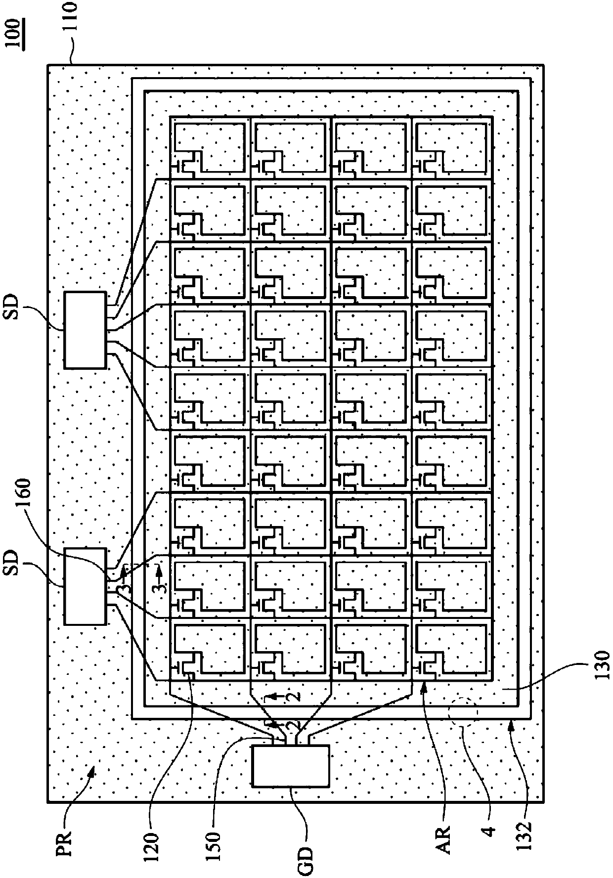
[0076] figure 1 A top view of the active device array substrat...


PUM


Abstract

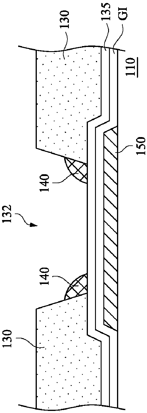
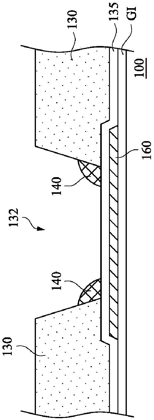
The invention provides an active component array substrate comprising a substrate body, a pixel circuit, a flat layer and a conductor pattern. The pixel circuit is arranged on the substrate body. The flat layer is arranged on the substrate body and at least partially overlaps the pixel circuit. The flat layer is provided with a groove, and the groove is arranged on the periphery of the substrate body and surrounds the pixel circuit. At least one side, adjacent to the groove, of the flat layer is provided with a cutting structure. The conductor pattern is arranged in at least part of the groove, is adjacent to the flat layer, and is provided with multiple discontinuous sections. A gap is formed between every two adjacent sections, and the gaps correspond to the cutting structure of the flat layer. The side, adjacent to the groove, of the flat layer is provided with the cutting structure, so that an electrical problem caused by residual metal can be avoided.

Description

technical field [0001] The invention relates to an active element array substrate. Background technique [0002] With the continuous development of display technology, in response to the needs of future displays, including light and thin, strong, portable, easy to read information and multi-functional integration, etc., flat-panel displays are gradually replacing traditional displays. Combined with the future life situation, the smart life style will emphasize interaction and connection, personalization and the convenience of obtaining information. Various products of flat-panel displays, such as notebook computers, monitors, monitors, TVs and e-books, will be Appearing more and more widely beside you and me. [0003] In general flat-panel displays, the material of the flat layer is mostly organic material, which has the characteristic of absorbing water vapor, so the water vapor will be transported into the display area through the flat layer, deteriorating the internal me...

Claims


Application Information

Patent Timeline
Patent Type & Authority Patents(China)
IPC IPC(8): H01L27/12
CPCH01L27/124H01L27/1248
Inventor 周政盈
Owner AU OPTRONICS CORP
Learn More