Electronic devices with high static protection

An electronic device and electrical connection technology, applied in the direction of electrical digital data processing, input/output process of data processing, instruments, etc., can solve the problems of reducing the utilization rate of substrate surface area, increasing lens manufacturing materials, increasing costs, etc., to achieve saving The effect of making materials, increasing the utilization rate of surface area, and increasing the electrostatic protection ability

Active Publication Date: 2018-03-27
PIXART IMAGING INC
View PDF4 Cites 0 Cited by
  • Summary
  • Abstract
  • Description
  • Claims
  • Application Information

AI Technical Summary

Problems solved by technology

However, the use of large-size lenses will increase the lens manufacturing materials and increase the cost
[0006] In addition, since the circuit board 90 has the circuit board opening 904, the electrical traces on the circuit board 90 can only be arranged on the remaining substrate surface, thereby reducing the utilization rate of the substrate surface area.

Method used


Image

  • Electronic devices with high static protection
  • Electronic devices with high static protection
  • Electronic devices with high static protection

Examples


Embodiment Construction

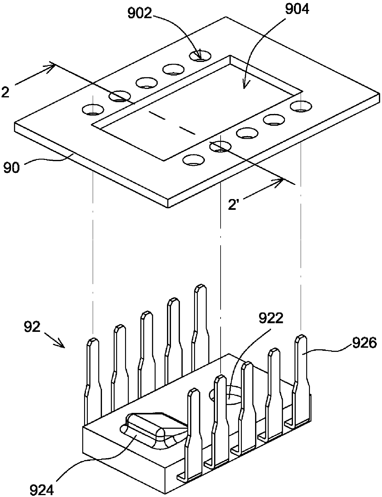
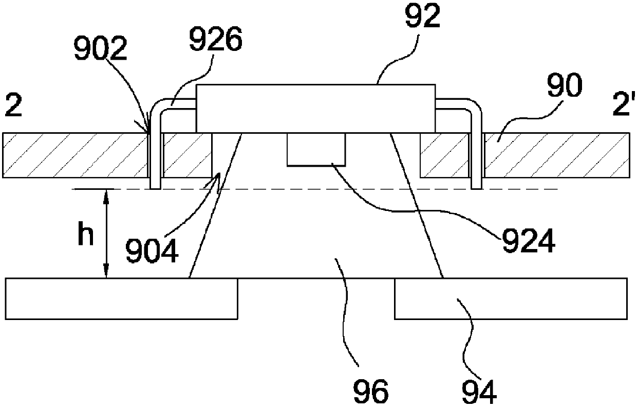
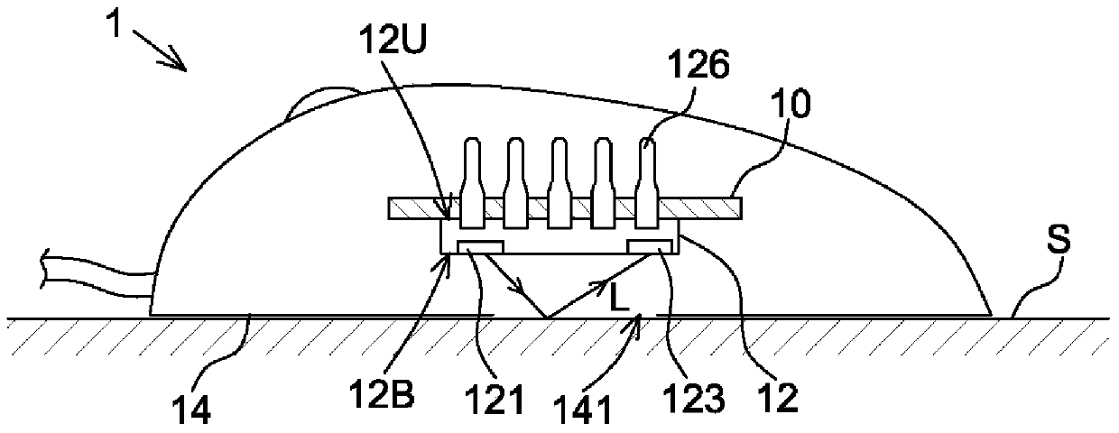
[0053] Please refer to image 3 , which shows a schematic diagram of an electronic device 1 according to an embodiment of the present invention. It must be noted that although an optical mouse is used as an example here, the present invention is not limited thereto. The electronic device 1 can also be portable electronic devices such as mobile phones, tablet computers, and optical navigation devices, which have functions A light source for illuminating the reflective surface and an image sensor for receiving reflected light from the reflective surface. For example, when the electronic device 1 is an optical mouse, the reflective surface can be a working surface S (such as image 3 shown); when the electronic device 1 is another portable device, such as a proximity sensor (proximity sensor), it can be used to detect the distance of an approaching object, so the reflective surface can be, for example, the surface of a finger or the surface of other objects .

[0054] Please a...


PUM


Abstract

The invention provides a high-static protection electronic device, which includes a substrate and a photoelectric element package. The photoelectric component package includes a light source, an image sensor and multiple leads. The light source is used to emit light toward the bottom surface of the photoelectric element package. The image sensor is used for receiving reflected light from the direction of the bottom surface. The pins are bent toward the opposite direction of the bottom surface to electrically connect the substrate, so as to increase the discharge path of the electrostatic discharge.

Description

technical field [0001] The invention relates to an electronic device, in particular to an electronic device capable of increasing the electrostatic protection capability of photoelectric elements and the utilization rate of substrate area. Background technique [0002] Optical mice typically contain an image sensor package that emits light as well as senses light. E.g figure 1 A schematic diagram of an image sensor package 92 and a circuit board 90 included in a known optical mouse is shown. The image sensor package 92 includes a light emitting diode 922 , an image sensor 924 and a plurality of pins 926 . The circuit board 90 includes a plurality of metal holes 902 and a circuit board opening 904 ; wherein the circuit board opening 904 is used for passing light. The image sensor packages 92 are respectively inserted into the metal holes 902 through the pins 926 to be combined with the circuit board 90 . [0003] When the optical mouse is placed on the work surface, the l...

Claims


Application Information

Patent Timeline
Patent Type & Authority Patents(China)
IPC IPC(8): G06F3/0354
Inventor 王聪法张彦闵钟庆霖
Owner PIXART IMAGING INC
Why Eureka
Try Eureka