Display panel
A technology for display panels and surrounding areas, applied in static indicators, identification devices, instruments, etc., to solve problems such as limiting the application of display panels
- Summary
- Abstract
- Description
- Claims
- Application Information
AI Technical Summary
Problems solved by technology
Method used
Image

Examples
Embodiment Construction
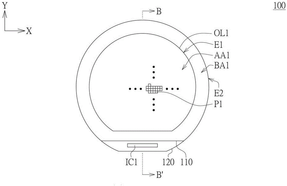
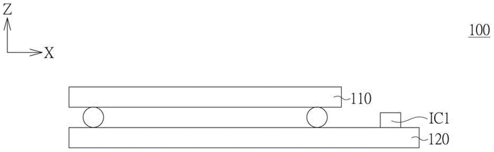
[0052] Please refer to Figure 1A and Figure 1B , Figure 1A It shows a display panel 100 according to an embodiment of the present invention, Figure 1B drawn along Figure 1A The cross-sectional view of the display panel 100 along the section line B-B'. The display panel 100 includes a first substrate 110 and a second substrate 120 . The first substrate 110 may be a color filter (color filter, CF) substrate. The second substrate 120 may be a thin film transistor (thin film transistor, TFT) array substrate. The second substrate 120 is larger than the first substrate 110 to provide a driving chip IC1.
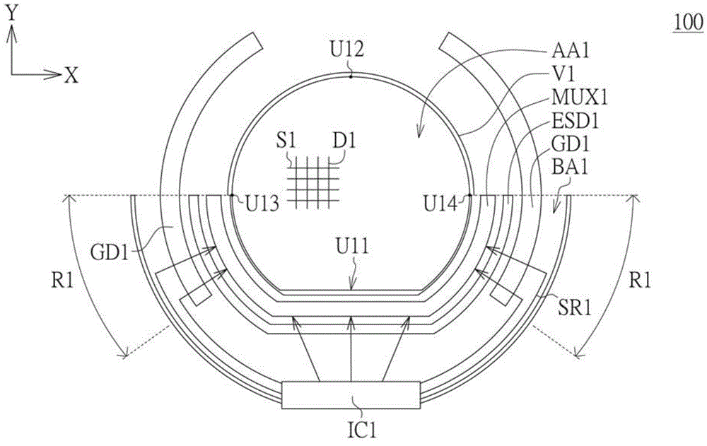
[0053] The display panel 100 has a pixel area AA1 and a peripheral area BA1. The pixel area AA1 is used for displaying images, and the peripheral area BA1 is used for setting lines. The peripheral area BA1 surrounds the pixel area AA1. In this embodiment, the overall outline OL1 of the pixel area AA1 is an arc, a polygon or a substantially round shape. A substantially c...
PUM
 Abstract
Description
Claims
Application Information
 - R&D Engineer
- R&D Manager
- IP Professional
- Industry Leading Data Capabilities
- Powerful AI technology
- Patent DNA Extraction
Browse by: Latest US Patents, China's latest patents, Technical Efficacy Thesaurus, Application Domain, Technology Topic.
© 2024 PatSnap. All rights reserved.Legal|Privacy policy|Modern Slavery Act Transparency Statement|Sitemap