
Method for producing a three-dimensional circuit configuration and circuit configuration

A circuit device, three-dimensional technology, applied in the field of manufacturing three-dimensional circuit devices, injection molding circuit devices, can solve problems such as expensive

Inactive Publication Date: 2015-10-14
ROBERT BOSCH GMBH
View PDF8 Cites 2 Cited by
  • Summary
  • Abstract
  • Description
  • Claims
  • Application Information

AI Technical Summary

Problems solved by technology

[0006] Such methods generally only allow relatively specific configurations of circuit arrangements and are somewhat expensive

Method used


Image

  • Method for producing a three-dimensional circuit configuration and circuit configuration
  • Method for producing a three-dimensional circuit configuration and circuit configuration
  • Method for producing a three-dimensional circuit configuration and circuit configuration

Examples


Embodiment Construction

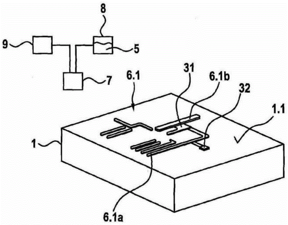
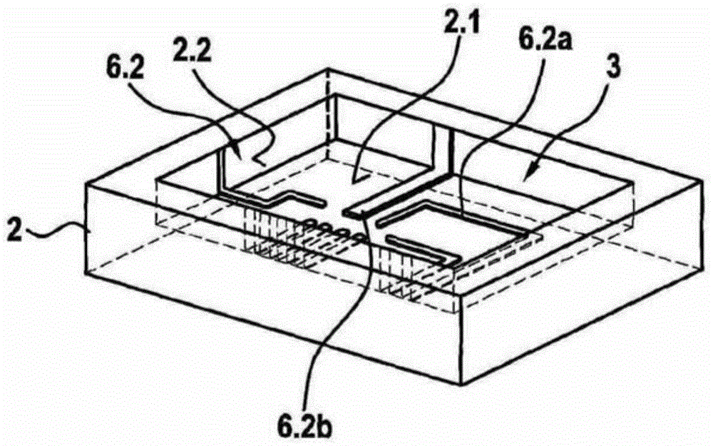
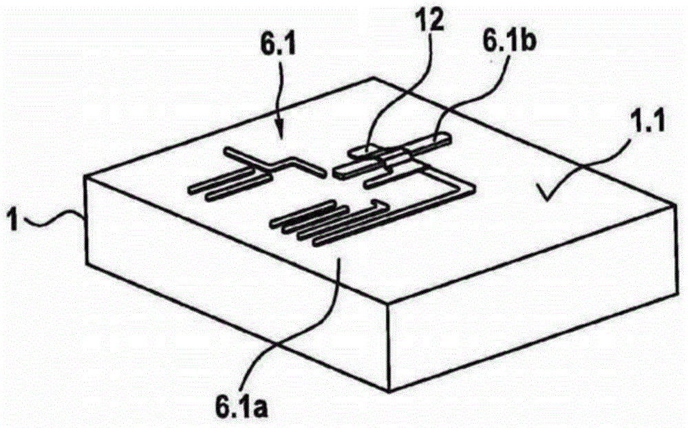
[0027] Figure 1a and 1b Two injection molding tools 1 , 2 are shown, wherein the first injection molding tool 1 is embodied as a cuboid and the second injection molding tool 2 is embodied as a cuboid with a recess 3 . The edge lengths of the base surfaces of the two injection molding tools 1 , 2 are approximately the same, so that the two injection molding tools 1 , 2 can be placed flush with each other. The surfaces 1.1, 2.1 and sides 2.2 of the injection molding tools 1, 2, which are embodied as active surfaces, define the shape of the injection molded circuit arrangement 4 to be produced, that is to say they form the "cathode" of the injection molded circuit arrangement 4, which molding circuit device 4 in Figure 4 and 5 Two examples are shown in . The two shown injection molding tools 1 , 2 here represent only simple embodiments; however, it is also possible to use more than two injection molding tools, for example with a plurality of steps and recesses, in order to o...


PUM


Abstract

A method for producing a three-dimensional, injection-molded circuit configuration includes: providing at least two injection molds, in each case having at least one effective surface; applying an electrically conductive material on at least one of the effective surfaces of at least one of the injection molds, while forming electrically conductive patterns; forming a hollow space bounded by the effective surfaces of the at least two injection molds; introducing an insulating material into the hollow space using an injection molding process, and forming a circuit substrate completely or partially accommodating the conductive patterns; and removing from the injection molds the injection-molded circuit configuration having the conductive patterns and the circuit substrate.

Description

technical field [0001] The invention relates to a method for producing a three-dimensional circuit arrangement, in particular an injection-moulded circuit arrangement, and to a circuit arrangement producible thereby. Background technique [0002] The manufacture of three-dimensional injection-molded circuit arrangements that are spatially extended, so-called MID circuit arrangements (Molded Interconnect Devices, MIDs), generally takes place in several steps. First, the circuit carrier is produced in an injection molding process, for example with a plurality of steps or recesses. Conductive structures are then applied to the surface of the circuit carrier, which are later used, for example, as conductor tracks or connection structures or contact structures. For example, individual elements can be electrically connected to each other via these electrically conductive structures. [0003] For this purpose, PCK (printed circuit board kollmorgen: printed circuit board Kollmorge...

Claims


Application Information

Patent Timeline
Patent Type & Authority Applications(China)
IPC IPC(8): H05K3/00H05K3/20
CPCH05K3/101H05K1/0284H05K1/092H05K1/11H05K1/182H05K3/0014H05K3/207H05K2201/09118
Inventor P·狄塞耳M·温克勒R·亨格勒M·施利茨库斯
Owner ROBERT BOSCH GMBH
Learn More