One-dimensional cascaded plasma photonic crystal and omnibearing band gap maximization design method thereof

A plasmonic and photonic crystal technology, applied in the field of one-dimensional cascaded plasmonic photonic crystal and its omnidirectional bandgap maximization design

Inactive Publication Date: 2015-11-04
SHANGHAI UNIV
View PDF8 Cites 7 Cited by
  • Summary
  • Abstract
  • Description
  • Claims
  • Application Information

AI Technical Summary

Problems solved by technology

[0005]Prior technology [2] (see Physics Letters A, 2014, 378(18), 1326–1332) produces omnidirectional bandgap for one-dimensional ternary photonic crystal The conditions for this technology are described in detail, but the method discussed in this technique is only applicable to one-dimensional photonic crystals of general conventional materials (the refractive index of such photonic crystal materials is constant), and for photonic crystals composed of other special materials, such as Plasma photonic crystals, due to the particularity of the plasma material, its dielectric constant changes with the frequency, so the situation that the refractive index of the material also changes with the frequency is not applicable

Method used


Image

  • One-dimensional cascaded plasma photonic crystal and omnibearing band gap maximization design method thereof
  • One-dimensional cascaded plasma photonic crystal and omnibearing band gap maximization design method thereof
  • One-dimensional cascaded plasma photonic crystal and omnibearing band gap maximization design method thereof

Examples


Embodiment 1

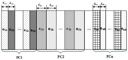
[0023] see figure 1 , the one-dimensional cascaded plasmonic photonic crystal is composed of dielectric layers and plasma layers alternately stacked, and is characterized in that: making full use of multiple band gaps of PC, by making n bands of PCs cascaded in n phases The gap can be connected to each other for all polarization states of TM and TE in all incident angle ranges. For all polarization states of TM and TE in all incident angle ranges, the lower limit of the first band gap of PC2 is connected with the upper limit of the first band gap of PC1, and the upper limit of the first band gap of PC2 is connected with the upper limit of PC1 The lower limit of the second band of PC2 is connected with the upper limit of the second band of PC1, the upper limit of the second band of PC2 is connected with the third band of PC1 The lower limit is connected, and so on to n-level PC, n is a natural number except zero.

Embodiment 2

[0025] The omni-directional bandgap maximization design method of the above-mentioned one-dimensional cascaded plasmonic photonic crystal is characterized in that the specific design steps are:

[0026] (1) According to the known structural parameters of the previous PC, the upper and lower limits of the first, second, ..., nth band gaps are obtained at normal incidence;

[0027] (2) According to the fact that multiple band gaps of cascaded PCs can be connected to each other, determine the upper and lower limits of the first band slot, the second band slot, ..., the nth band slot of the next PC at normal incidence location area;

[0028] (3) Adjust the structural parameters of the latter PC, and preliminarily determine the structural parameters of the latter PC by making the position of each band gap of the latter PC meet the upper and lower limit position areas of each band gap determined in the previous step;

[0029] (4) Judging whether the light of all polarization s...

Embodiment 3

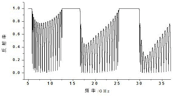
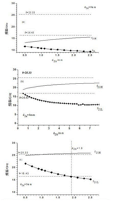
[0031] Take the cascaded structure of two plasma PCs as an example to illustrate the design of the maximum omni-directional bandgap based on the method of the present invention. The structure is as attached figure 1 shown. Here, the periods of the a and b media in PC1 and PC2 are selected as 20; the a media is a dielectric material with a refractive index of 2, and the a media of the two PCs are the same, that is, n 2a =n 1a =2; the b medium of the two PCs is also the same, that is, the dielectric constant of the b medium of PC1 e 1b and the dielectric constant of the b medium of PC2 e 2b for , where the electron plasma frequency , the collision frequency , w is the angular frequency of the incident light. The refractive index of medium b in PC1 and PC2 is then . Angular frequency of incident light w and incident light frequency f The relationship is w =2p f . Known a dielectric thickness d of PC1 1a =5mm, realize the omnidirectional reflector with maxim...


PUM


Abstract

The invention relates to a one-dimensional cascaded plasma photonic crystal and an omnibearing band gap maximization design method thereof. The multiple band gaps of cascaded photonic crystals may mutually connect in all TM polarization state light and TE polarization state light in all incident angle ranges. The design method is suitable for plasma photonic crystal cascaded structure. An omnibearing reflector designed by using the method has a maximum omnibearing photon band gap.

Description

technical field [0001] The invention relates to a design method for enlarging the omni-directional bandgap of a one-dimensional photonic crystal, which is especially suitable for cascade-structured one-dimensional plasma photonic crystals and a design method for maximizing the omnidirectional bandgap, so as to achieve the largest omnidirectional bandgap omnidirectional reflector. Background technique [0002] In the late 1980s, John and Yablonovitch first proposed the concept of photonic crystal (PC) internationally. Photonic crystal is a periodic artificial dielectric structure with the same order of magnitude as the wavelength. Due to its unique photon band gap and photon localization characteristics, it has quickly become a research hotspot for researchers. It is used in filters, lasers, Optical switches and many other fields have a wide range of applications. Through rational design, the photonic crystal will have a photonic band gap that prohibits the transverse elect...

Claims


Application Information

Patent Timeline
Patent Type & Authority Applications(China)
IPC IPC(8): G02B6/122
CPCG02B6/1225G02F2202/32
Inventor 张娟邹俊辉华东
Owner SHANGHAI UNIV
Why Eureka
Try Eureka