Method of making a stacked package

A packaging and stacking technology, which is applied in the field of stacked packaging and its manufacturing method, can solve the problems of cleaning device reducing cleaning effect, easy access, damage to the second substrate, etc.

Active Publication Date: 2018-02-02
SILICONWARE PRECISION IND CO LTD
View PDF3 Cites 0 Cited by
  • Summary
  • Abstract
  • Description
  • Claims
  • Application Information

AI Technical Summary

Problems solved by technology

[0009] Please refer to Figure 1B , because in another existing manufacturing process embodiment of a stacked package, the singulated second substrate 30 is placed on the first substrate 10 that is still formed into a layout structure, and the first substrate 10 and the second substrate 30 The first encapsulant 16 is formed between them. When cutting the typesetting structure with the cutter 6, if the area of ​​the upper and lower substrates is the same, the cutter 6 will easily contact the second substrate 30, thereby forming a moment on the second substrate 30, damage the second substrate 30
[0010] Therefore, how to overcome the problem that the cleaning effect of the existing stacked package with the same area of ​​the upper and lower substrates is hindered by the upper substrate and reduce the cleaning effect, and how to overcome the problem that the second substrate is affected by the tool when cutting the layout structure. The problem of damage caused by applying force is actually a big problem for those skilled in the art

Method used


Image

  • Method of making a stacked package
  • Method of making a stacked package
  • Method of making a stacked package

Examples


Embodiment Construction

[0058] The implementation of the present invention will be described below through specific specific examples, and those skilled in the art can easily understand other advantages and effects of the present invention from the content disclosed in this specification. The present invention can also be implemented or applied through other different specific embodiments, and various modifications and changes can be made to the details in this specification based on different viewpoints and applications without departing from the spirit of the present invention.

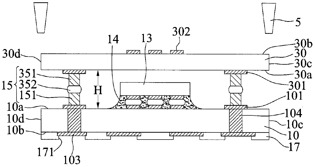
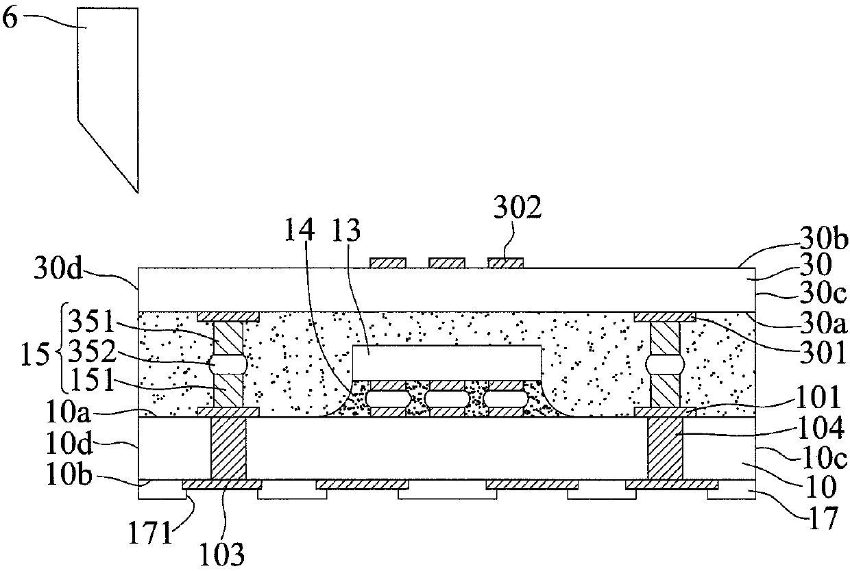
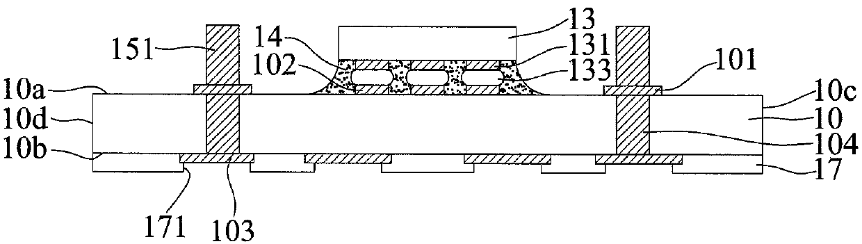
[0059] Please refer to Figure 2A to Figure 2D and Figure 2A 'and Figure 2B ’, these figures are a cross-sectional view and a top view of the first embodiment of the manufacturing method of the stacked package of the present invention, wherein each step of the manufacturing method of the stacked package will be described in detail below with reference to each figure.

[0060] Please refer to Figure 2A , Figure 2A ’...


PUM


Abstract

A stacked package and its manufacturing method, the package comprising: a first surface and a second surface opposite to each other, a first side surface and a second side surface opposite to each other connecting the first surface and the second surface, and A first substrate with a plurality of first electrical connection pads; a chip electrically connected to the first surface; connected to the first surface of the first substrate and having opposite third and fourth surfaces , the second substrate connecting the third surface and the fourth surface and the opposite third side surface and the fourth side surface, a plurality of second electrical connection pads, the distance between the third side surface and the fourth side surface 15 to 3900 microns smaller than the distance between the first side surface and the second side surface; and corresponding to a plurality of interconnection structures electrically connecting the first electrical connection pad and the second electrical connection pad. The invention can improve the cleaning effect of the cleaning device and reduce the damage probability of the second substrate caused when cutting the first typesetting structure.

Description

technical field [0001] The invention provides a stacked package and its manufacturing method, in particular to a stacked package with different substrate areas on the upper and lower layers and its manufacturing method. Background technique [0002] Due to the popularity of portable electronic devices, more and more electronic devices need to be light, thin and compact, especially for semiconductor components and their packaging structures, which are constantly pursuing smaller and thinner designs. Therefore, the technology of stacked packages is also thereby flourishing. [0003] Please refer to Figure 1A and Figure 1B , which is a cross-sectional view of an existing stacked package with the same upper and lower substrate areas, where, Figure 1A and Figure 1B The stacked package includes a first substrate 10, a chip 13, a second substrate 30, and a plurality of interconnect structures 15, and also includes a primer 14 and an insulating protective layer 17. The area of...

Claims


Application Information

Patent Timeline
Patent Type & Authority Patents(China)
IPC IPC(8): H01L25/00H01L23/31H01L23/488H01L21/50
CPCH01L2224/16225H01L2224/32225H01L2224/73204H01L2224/97H01L2924/15311H01L2924/181
Inventor 黄淑惠江政嘉王隆源施嘉凯徐逐崎
Owner SILICONWARE PRECISION IND CO LTD
Why Eureka
Try Eureka