Array substrate and driving method thereof

An array substrate and driving voltage technology, applied in nonlinear optics, static indicators, instruments, etc., can solve the problems of W sub-pixel brightness changes, enhanced capacitive coupling effects, poor viewing experience, etc., to achieve reduced brightness changes, reduced The effect of reducing the brightness of small screen brightness and reducing the effect

Active Publication Date: 2015-11-11
TCL CHINA STAR OPTOELECTRONICS TECH CO LTD
View PDF5 Cites 22 Cited by
  • Summary
  • Abstract
  • Description
  • Claims
  • Application Information

AI Technical Summary

Problems solved by technology

However, in the driving of the liquid crystal display panel with the above-mentioned RGBW pixel structure, the voltage polarity of the W sub-pixel and the R sub-pixel will be the same, that is, the polarities of D4 and D5 of the adjacent data lines on both sides of the W sub-pixel are the same, The capacitive coupling effect of the data line to the pixel electrode of the W sub-pixel is strengthened, thereby changing the voltage of the pixel electrode of the W sub-pixel, that is, vertical crosstalk is generated, resulting in a change in the brightness of the W sub-pixel
The W sub-pixel usually displays white to compensate for the brightness of the screen and has high brightness. Therefore, a slight change in the gray scale of the W sub-pixel will lead to a large change in brightness, making it easier for the human eye to perceive the change in brightness, resulting in The viewing experience of poor picture quality

Method used


Image

  • Array substrate and driving method thereof
  • Array substrate and driving method thereof
  • Array substrate and driving method thereof

Examples


Embodiment Construction

[0026] The present invention will be described in detail below with reference to the drawings and embodiments.

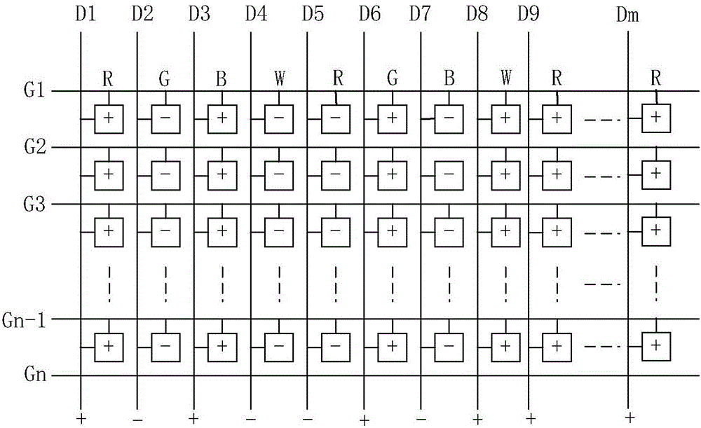
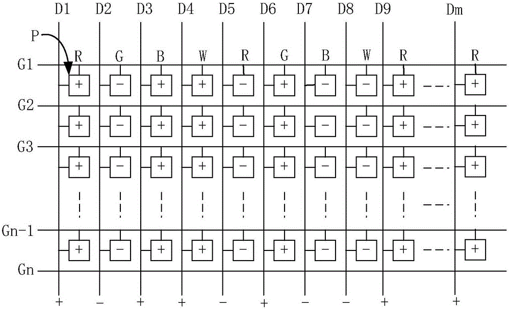
[0027] refer to image 3 , In an embodiment of the array substrate of the present invention, the array substrate is an array substrate in a liquid crystal display panel, and the array substrate includes a plurality of scanning lines G1 to Gn (n greater than or equal to 1) arranged along the row direction, and a plurality of scanning lines G1 to Gn arranged along the column direction. Data lines D1˜Dm (m greater than or equal to 1) and a plurality of sub-pixels P arranged in an array defined by the scan line Gn and the data line Dm, each sub-pixel P is respectively connected to a scan line Gn and a data line Dm. A plurality of scanning lines G1-Gn and a plurality of data lines D1-Dm are located in the opaque area of ​​the array substrate, that is, the scanning lines and data lines are arranged corresponding to the black matrix on the color filter substrate of the liq...


PUM


Abstract

The invention discloses an array substrate and a driving method thereof. The array substrate comprises a plurality of scanning lines arranged along a row direction, a plurality of data lines arranged along a column direction and a plurality of sub-pixels which are defined by the scanning lines and the data lines and are arranged in an array mode. The plurality of sub-pixels are divided into a plurality of sub-pixel columns with different colors, wherein the plurality of sub-pixel columns are arranged periodically along the row direction. At least one sub-pixel column is a compensation light sub-pixel column. In a same picture frame, driving voltage polarities on adjacent data lines of two sides of the compensation light sub-pixel column are opposite. Through the above mode, picture brightness changes can be reduced and picture quality is increased.

Description

technical field [0001] The invention relates to the technical field of liquid crystal display, in particular to an array substrate and a driving method thereof. Background technique [0002] Compared with the traditional RGB pixel structure liquid crystal display panel, the RGBW pixel structure liquid crystal display panel has a higher transmittance due to the addition of W sub-pixels (white pixels) as compensation photon sub-pixels, which can reduce backlight power consumption , so as to reduce costs and have better development prospects. [0003] Such as figure 1 As shown, in the existing liquid crystal display panel with RGBW pixel structure, each pixel unit includes R sub-pixel, G sub-pixel, B sub-pixel and W sub-pixel, R sub-pixel, G sub-pixel, B sub-pixel and W sub-pixel The pixels are arranged sequentially along the row direction. A plurality of scanning lines G1-Gn are arranged in sequence along the column direction, and a plurality of data lines D1-Dn are arrange...

Claims


Application Information

Patent Timeline
Patent Type & Authority Applications(China)
IPC IPC(8): G09G3/36
CPCG09G3/3614G09G3/3648G09G2300/0452G02F1/133512G02F1/133514G02F1/136286G09G3/2003G09G3/2074G09G3/3677G09G3/3688G09G3/3696G09G2320/0646G09G2320/0666
Inventor 何涛陈宥烨何振伟
Owner TCL CHINA STAR OPTOELECTRONICS TECH CO LTD
Why Eureka
Try Eureka